Introduction
Designing a high current power supply demands precision and a deep understanding of printed circuit board (PCB) engineering to ensure reliability and performance. Thick copper PCBs are essential in such applications due to their ability to handle substantial current loads while minimizing thermal issues. This guide, tailored for electric engineers, explores the intricacies of PCB design, component selection, layout strategies, and testing methodologies for high current power supplies. By following a structured approach, engineers can mitigate risks like overheating and voltage drops. The focus will be on practical steps to achieve efficient power delivery using thick copper layers, adhering to recognized industry standards for quality and safety. Whether you are refining an existing design or starting anew, this article provides actionable insights for success.
What Are High Current Power Supplies and Why Use Thick Copper PCBs
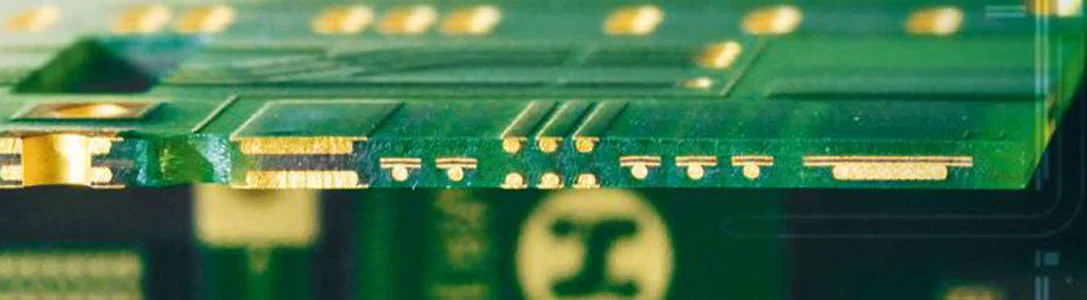
High current power supplies are systems designed to deliver significant electrical current, often exceeding several amperes, to support demanding applications like industrial machinery, electric vehicle chargers, and server systems. These supplies must maintain stable voltage levels under heavy loads, making the underlying PCB design critical. Thick copper PCBs, typically featuring copper layers with thicknesses of 2 ounces per square foot or more, offer enhanced current carrying capacity and improved heat dissipation compared to standard boards.
The primary reason for using thick copper lies in its ability to reduce resistive losses. Higher current densities in thinner copper layers lead to increased heat generation, risking component failure. Thick copper mitigates this by providing a lower resistance path, ensuring efficient power transfer. Additionally, it enhances mechanical strength, which is vital for boards subjected to thermal cycling or physical stress. For engineers, adopting thick copper in high current designs is not just a preference but a necessity to meet performance and safety requirements.
Related Reading: Heavy Copper PCB: An overview of its benefits and applications
Technical Principles of High Current PCB Design with Thick Copper
Understanding the principles behind high current PCB design starts with recognizing the relationship between current, resistance, and heat. According to Ohm’s Law, voltage drop across a conductor increases with current and resistance. In PCB traces, resistance is influenced by copper thickness, trace width, and length. Thick copper layers reduce resistance, allowing higher current flow without excessive voltage drops or thermal buildup.
Thermal management is another critical aspect. High currents generate heat through Joule heating, which can degrade components or delaminate the PCB if not addressed. Thick copper acts as a heat sink, spreading thermal energy across the board. Engineers must also consider the current carrying capacity of traces, often guided by standards like IPC-2221B, which provides formulas and charts for determining safe trace widths based on current and temperature rise.
Dielectric materials between copper layers must withstand thermal and electrical stress. Selecting substrates with high thermal conductivity ensures heat dissipation, while maintaining dielectric strength prevents breakdowns under high voltage conditions. These principles form the foundation for designing robust high current power supplies, ensuring both electrical performance and long term reliability.
Step by Step Guide to Building a High Current Power Supply
Step 1: Define Specifications and Requirements
Begin by outlining the power supply’s electrical requirements, including output voltage, maximum current, and load characteristics. Determine the acceptable voltage drop and temperature rise for your application. These specifications will guide the selection of copper thickness and trace dimensions. Ensure compliance with relevant standards such as IPC-6012E for rigid board performance to guarantee quality and durability.
Step 2: Select Thick Copper PCB Specifications
Choose a copper thickness suitable for the expected current load. For high current applications, copper weights of 3 to 6 ounces per square foot are common. Consult guidelines from IPC-2221B to calculate minimum trace widths based on current and allowable temperature rise. Opt for a substrate material with high thermal conductivity to aid heat dissipation. Verify that the board manufacturer can support the chosen copper thickness and layer stack up.
Step 3: Component Selection for High Current Loads
Select components rated for the anticipated current and voltage levels. Power MOSFETs, diodes, and capacitors must have low on state resistance and high thermal tolerance. Inductors and transformers should minimize core losses at high currents. Ensure that component footprints align with thermal vias and copper planes for optimal heat transfer. Adhering to standards like JEDEC J-STD-020E for moisture sensitivity during assembly prevents component damage.
Step 4: PCB Layout Strategies for High Current
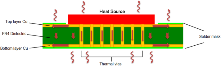
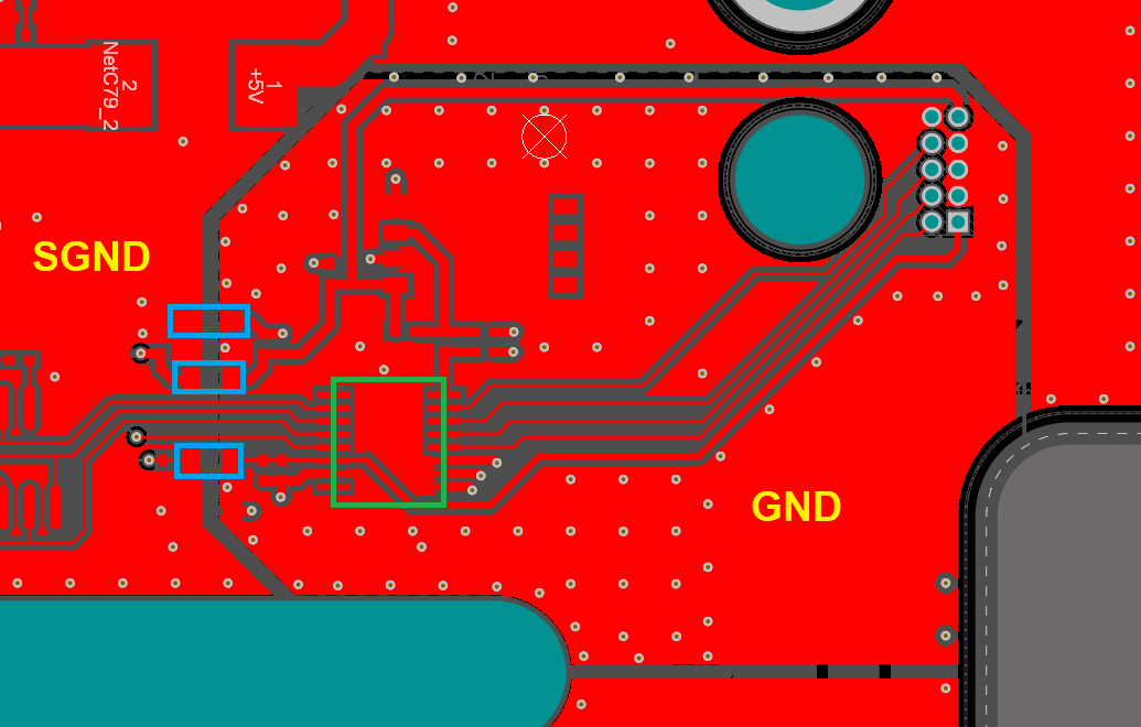
Layout design is pivotal in managing current distribution and thermal performance. Place high current traces on outer layers with thick copper to minimize resistance. Use wide traces or copper pours for power paths to reduce inductance and voltage drops. Position components to shorten trace lengths, especially for critical paths. Incorporate thermal vias near heat generating components to transfer heat to inner or bottom layers. Separate high current paths from sensitive signal traces to avoid electromagnetic interference.
Step 5: Power Plane Design and Grounding
Implement dedicated power and ground planes to provide low impedance paths for current flow. Thick copper planes enhance current capacity and act as heat spreaders. Ensure multiple vias connect power planes to component pads for uniform current distribution. A solid ground plane reduces noise and provides a return path for currents. Follow best practices from IPC-A-600K for acceptable board design to ensure manufacturability and performance.
Step 6: Thermal Management Techniques
Incorporate thermal relief structures around pads to balance heat distribution during soldering. Use heat sinks or forced air cooling for critical components if passive dissipation via thick copper is insufficient. Simulate thermal profiles using design tools to identify hotspots. Ensure that the board’s thermal design aligns with guidelines from IPC-2221B to prevent overheating under load conditions.
Step 7: Testing the High Current Power Supply
Testing validates the design’s performance under real world conditions. Begin with a visual inspection per IPC-A-600K standards to check for manufacturing defects. Conduct electrical tests to measure voltage drops across traces and verify current handling capacity. Use thermal imaging to identify overheating areas during load testing. Apply full load conditions to simulate operational stress, monitoring for stability and efficiency. Document results to ensure compliance with initial specifications.
Related Reading: Heavy Copper Handling: Designing PCBs for High-Power Industrial Applications
Common Challenges and Troubleshooting Tips
High current designs often face challenges like trace overheating, component failure, and unexpected voltage drops. Overheating can result from insufficient copper thickness or poor thermal via placement. Address this by increasing copper weight or adding more vias for heat transfer. Component failures may occur due to underrated parts; always verify specifications against load requirements. Voltage drops indicate inadequate trace width or length, which can be resolved by consulting IPC-2221B charts for adjustments.
Electromagnetic interference is another concern, often caused by high current loops near sensitive signals. Minimize loop areas and use shielding or ground planes to reduce noise. If issues persist during testing, systematically isolate variables like load current or ambient temperature to pinpoint root causes. Keeping detailed records of design iterations and test outcomes aids in refining future projects for optimal performance.
Conclusion
Building a high current power supply with thick copper PCBs requires meticulous attention to design principles, component selection, layout strategies, and rigorous testing. By leveraging thick copper layers, engineers can effectively manage high current loads while mitigating thermal risks. This step by step guide provides a structured approach to achieving reliable power delivery, grounded in industry standards for quality assurance. Applying these insights ensures that your power supply design meets performance expectations and withstands operational demands. With careful planning and adherence to best practices, success in high current applications is within reach.
FAQs
Q1: How does copper thickness impact high current power supply performance?
A1: Copper thickness directly affects the current carrying capacity and thermal performance of a PCB in a high current power supply. Thicker copper reduces resistance, minimizing voltage drops and heat generation under load. This ensures stable operation and prevents overheating, which can damage components. Standards like IPC-2221B offer guidance on selecting appropriate thicknesses based on current requirements for reliable designs.
Q2: What are key considerations for PCB layout in high current designs?
A2: In high current PCB design, layout is critical for efficiency and safety. Prioritize wide traces and copper pours for power paths to lower resistance. Place components to minimize trace lengths and use thermal vias for heat dissipation. Separate high current paths from sensitive signals to avoid interference. Following layout guidelines ensures optimal current flow and thermal management.
Q3: Why is testing crucial for high current power supply PCBs?
A3: Testing validates the reliability of a high current power supply PCB under operational conditions. It identifies issues like voltage drops, overheating, or component stress before deployment. Electrical and thermal tests ensure the design meets specifications and standards such as IPC-A-600K. Thorough testing prevents failures in real world applications, safeguarding performance and longevity of the power supply.
Q4: How can thermal issues be managed in high current PCB designs?
A4: Thermal management in high current PCB designs involves using thick copper layers to spread heat and incorporating thermal vias near heat generating components. Selecting substrates with high thermal conductivity aids dissipation. Additional cooling methods like heat sinks can be applied if needed. Adhering to IPC-2221B guidelines helps predict and mitigate thermal risks effectively.
References
IPC-2221B — Generic Standard on Printed Board Design. IPC, 2012.
IPC-6012E — Qualification and Performance Specification for Rigid Printed Boards. IPC, 2020.
IPC-A-600K — Acceptability of Printed Boards. IPC, 2020.
JEDEC J-STD-020E — Moisture/Reflow Sensitivity Classification for Nonhermetic Surface Mount Devices. JEDEC, 2014.


