Introduction
For electronic hobbyists venturing into printed circuit board design, understanding the intricacies of inner layer copper pouring can elevate the quality and performance of their projects. Copper pouring, a technique used to fill unused areas of a PCB with copper, plays a vital role in managing electromagnetic interference, enhancing heat dissipation, and improving structural integrity. When applied to inner layers of multilayer boards, it becomes even more critical for maintaining signal integrity and creating effective DIY ground planes. This article aims to break down the concept of PCB copper pouring with a focus on inner layer design. It provides practical insights and best practices tailored for hobbyists eager to refine their skills in crafting reliable and efficient circuit boards.
What Is Inner Layer Copper Pouring and Why It Matters
Inner layer copper pouring refers to the process of filling vacant areas on the internal layers of a multilayer PCB with copper, typically connected to ground or power nets. Unlike surface layers, inner layers are embedded within the board, making them ideal for creating stable reference planes such as ground or power planes. For hobbyists, this technique is essential when designing boards with more than two layers, as it helps manage electrical noise and supports high-speed signals.
The importance of inner layer copper pouring lies in its ability to reduce electromagnetic interference and crosstalk between traces. A well-designed ground plane on an inner layer acts as a shield, providing a low-impedance path for return currents. Additionally, it aids in heat distribution across the board, preventing localized hot spots during operation. For DIY enthusiasts, mastering this aspect of PCB design ensures better performance in projects involving microcontrollers, RF circuits, or power electronics.
Technical Principles of Inner Layer Copper Pouring
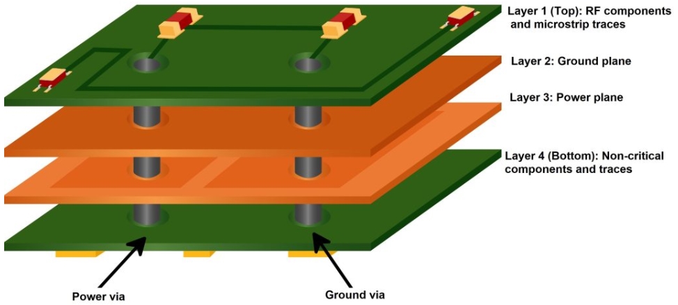
Copper pouring on inner layers follows the same fundamental principle as on outer layers: unused space is filled with copper to connect to a specific net, often ground. However, inner layers require careful consideration due to their role in multilayer stackups. Most hobbyist boards with inner layers use a four-layer configuration, where inner layers are dedicated to ground and power planes. This setup isolates signal layers from interference and provides a consistent reference for signal return paths.
The primary mechanism behind copper pouring is to create a uniform plane that minimizes loop inductance. When signals travel through traces, return currents seek the path of least resistance, often through the nearest ground plane. A solid or near-solid copper pour on an inner layer ensures these currents flow smoothly without creating noise. Gaps or incomplete pours can disrupt this flow, leading to signal integrity issues.
Another key principle is thermal management. Copper is an excellent conductor of heat, and a poured plane on an inner layer can dissipate heat from components mounted on outer layers. This is particularly useful for hobbyists working on compact designs where heat buildup is a concern. Standards such as IPC-2221B, which provides guidelines for PCB design, emphasize the importance of balanced copper distribution to prevent thermal stress and board warpage.
Challenges in Inner Layer Design for Hobbyists
Designing inner layers with effective copper pouring poses unique challenges for hobbyists. Limited access to advanced design tools and fabrication constraints often restrict the ability to create complex multilayer boards. Many hobbyists start with basic four-layer designs, where improper copper pouring can lead to manufacturing issues like uneven etching or delamination.
One common challenge is maintaining copper balance between layers. Uneven copper distribution can cause mechanical stress during fabrication, leading to board warpage. Standards such as IPC-6012E highlight the need for symmetrical copper distribution to ensure structural integrity. Hobbyists must ensure that inner layer pours are mirrored or balanced with outer layers to avoid such problems.
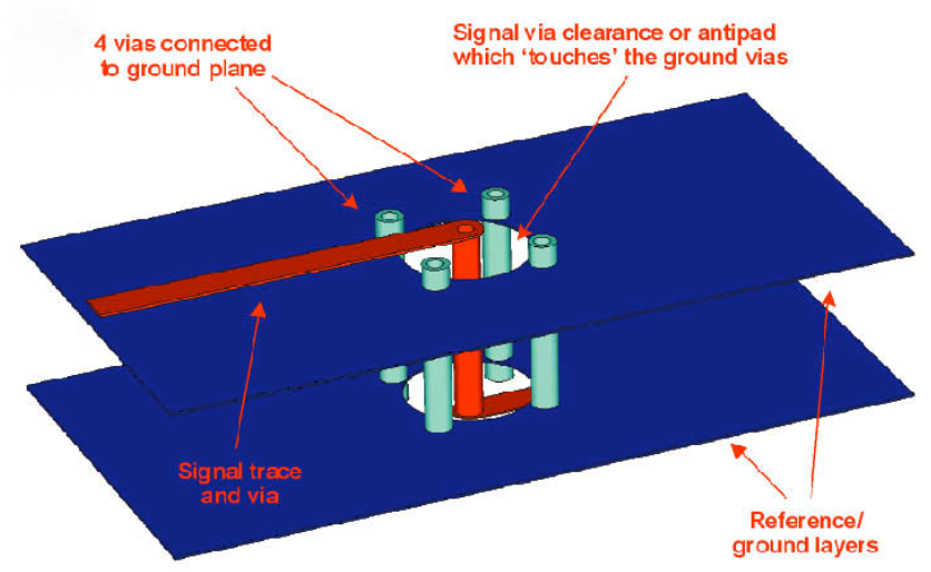
Another issue is via placement in relation to poured planes. Vias connect traces across layers, and if placed carelessly, they can interrupt the continuity of a ground plane. This creates isolated copper islands, which are problematic as they can act as antennas, picking up noise. Proper via stitching, where multiple vias connect planes across layers, helps maintain plane integrity.
Related Reading: The Ultimate Guide to Connecting Components with Inner Layer Traces
Best Practices for DIY Ground Planes and Copper Pouring
Creating effective DIY ground planes and copper pours on inner layers requires adherence to practical design principles. Hobbyists can achieve reliable results by following these best practices tailored to their typical tools and project scopes.
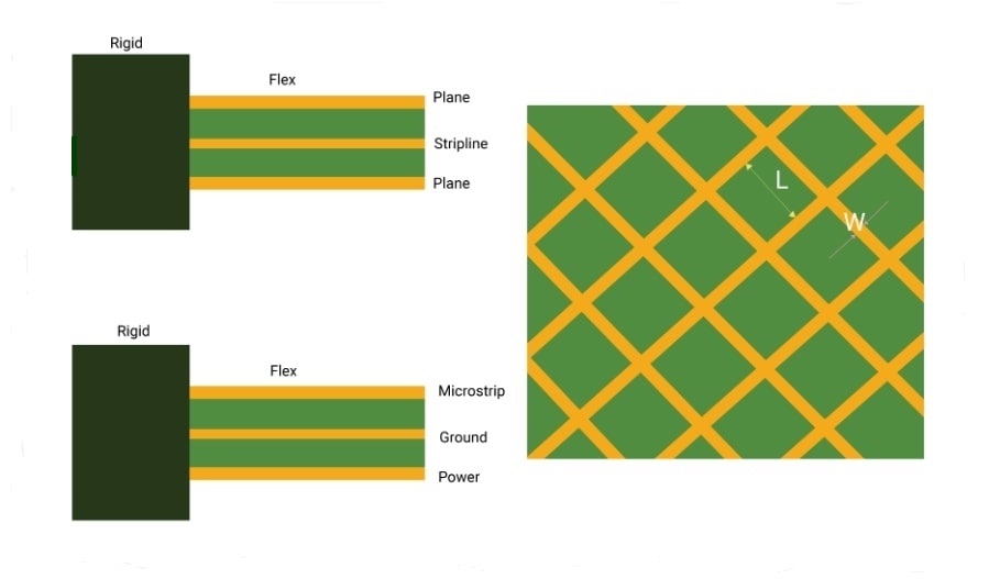
First, dedicate at least one inner layer to a solid ground plane in multilayer designs. In a four-layer board, assign the second layer as a ground plane and avoid routing traces on it. This ensures a continuous reference plane for signals on adjacent layers. If a power plane is needed, use the third layer and pour copper connected to the power net.
Second, minimize gaps in copper pours. While it might be tempting to leave empty spaces for aesthetic reasons, incomplete pours can disrupt return paths. Use design software features to fill areas automatically, ensuring connectivity to the intended net. Check for isolated copper islands after pouring and connect them with vias if necessary.
Third, balance copper across layers. If an inner layer has a dense pour, ensure other layers have similar copper coverage to prevent manufacturing defects. Refer to guidelines in IPC-2221B for achieving symmetry in multilayer stackups. This practice reduces the risk of warping during thermal cycles.
Fourth, use via stitching strategically around high-frequency signals or sensitive areas. Place vias at regular intervals along the edges of a ground plane to connect it to other ground layers. This technique, often recommended for EMI control, reinforces the plane’s shielding effect.
Finally, verify the design against manufacturing tolerances. Many hobbyist boards are fabricated through budget-friendly services with specific design rules. Ensure that copper pours do not violate minimum clearance or spacing requirements to avoid short circuits during production.
Related Reading: Ground plane for beginners: Making your first circuit!
Troubleshooting Common Issues in Inner Layer Copper Pouring
Hobbyists often encounter issues when implementing copper pouring on inner layers, especially due to limited experience with multilayer designs. One frequent problem is unintended isolation of copper areas. If a pour is not properly connected to the ground net, it becomes a floating plane, which can amplify noise. To resolve this, inspect the net assignment of each pour and add vias to tie isolated sections to the main plane.
Another issue is excessive copper removal during fabrication due to poor design rules. If traces or pads are too close to poured areas, etching processes might create unintended gaps. Always maintain adequate spacing as per fabrication guidelines to prevent such defects. Standards like IPC-A-600K provide criteria for acceptable board features and can guide hobbyists in identifying potential issues.
Thermal imbalance is also a concern. If an inner layer pour is significantly denser than others, it can lead to uneven heating during soldering or operation. Review the layer stackup and adjust pours to achieve uniform copper coverage. Simulation tools, if available, can help predict thermal behavior before fabrication.
Conclusion
Inner layer copper pouring is a powerful technique for electronic hobbyists looking to enhance the performance of their multilayer PCBs. By creating effective DIY ground planes and ensuring balanced copper distribution, hobbyists can significantly reduce noise, improve heat dissipation, and achieve reliable designs. Understanding the principles behind PCB copper pouring and following best practices tailored to inner layer design empowers enthusiasts to tackle complex projects with confidence. With careful planning and adherence to industry guidelines, even budget-conscious hobbyists can produce boards that rival professional standards in functionality and durability.
FAQs
Q1: What is PCB copper pouring, and why is it important for hobbyist designs?
A1: PCB copper pouring involves filling unused areas of a circuit board with copper, often connected to ground or power nets. For hobbyists, it is crucial as it reduces electromagnetic interference, improves signal integrity, and enhances heat dissipation. Properly poured inner layers act as stable reference planes, making designs more reliable, especially in multilayer boards with high-speed signals.
Q2: How can I create effective DIY ground planes on inner layers?
A2: To create DIY ground planes, dedicate an inner layer of your multilayer PCB to ground and avoid routing traces on it. Use design software to pour copper across the entire layer, ensuring it connects to the ground net. Add via stitching around critical areas to maintain continuity and minimize noise in your hobbyist projects.
Q3: What are common mistakes in inner layer design for hobbyist PCBs?
A3: Common mistakes include uneven copper distribution, leading to board warpage, and creating isolated copper islands that amplify noise. Hobbyists often overlook via placement, disrupting ground plane continuity. Following standards like IPC-2221B for balanced design and checking net connectivity can help avoid these issues in inner layer layouts.
Q4: How does inner layer copper pouring affect PCB manufacturing for hobbyists?
A4: Inner layer copper pouring impacts manufacturing by influencing board stability and etching uniformity. Balanced copper distribution, as recommended by IPC-6012E, prevents warping and ensures consistent fabrication. Hobbyists must adhere to design rules to avoid defects like short circuits, ensuring their boards meet basic quality expectations during production.
References
IPC-2221B — Generic Standard on Printed Board Design. IPC, 2012.
IPC-6012E — Qualification and Performance Specification for Rigid Printed Boards. IPC, 2020.
IPC-A-600K — Acceptability of Printed Boards. IPC, 2020.


