What Role Do Thermal Vias Play in PCB Design?
As electronic devices become more compact and powerful, effectively managing heat within printed circuit boards (PCBs) is increasingly critical. For those new to PCB design, ensuring components remain cool and preventing overheating is a key challenge. Thermal vias offer a straightforward yet highly effective solution for heat dissipation.
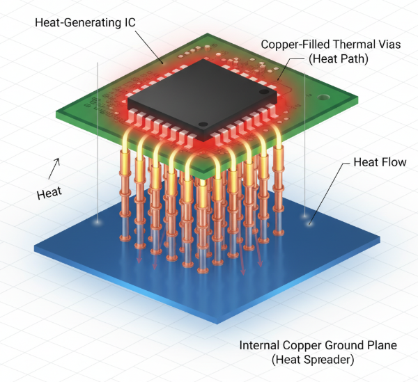
These small, specialized pathways within a PCB are designed specifically to transfer heat away from hot components toward cooler areas, such as a ground plane or a heat sink. Unlike standard vias, which route electrical signals between layers, thermal vias act like miniature heat conduits, moving thermal energy to prevent components from reaching damaging temperatures. They are fundamental to effective PCB heat management, typically positioned directly beneath or adjacent to heat-generating parts like power transistors, LEDs, or microprocessors to create an efficient escape route for heat.
Why Is Heat Management Crucial for PCB Performance?
Before delving deeper into the mechanics of thermal vias, it's important to understand why heat management is so vital in PCB design. Electronic components invariably produce heat during operation. If this heat isn't effectively managed and dissipated, it can lead to several significant issues.
Potential Issues from Inadequate Cooling
● Component Damage: Excessive heat can severely harm sensitive components, drastically shortening their operational life or causing immediate, catastrophic failure.
● Operational Problems: Elevated temperatures can reduce processor speeds or induce erratic and unpredictable behavior within circuits, compromising device reliability.
● Safety Concerns: In applications involving high power, overheating components can pose serious safety hazards, including fire risks.
Proper heat management ensures that your PCB operates within safe temperature thresholds, generally between 85°C and 125°C for most components, depending on their individual specifications. By employing strategies like thermal vias, designers can maintain optimal operating temperatures, thereby avoiding expensive redesigns or system failures.
Suggested Reading: Mastering Thermal Vias: Essential Heat Management for High-Power PCBs
How Do Thermal Vias Facilitate Heat Dissipation?
Thermal vias function by creating a direct, low-resistance pathway for heat to move from a hot spot on the PCB to a cooler zone. Standard PCB materials, such as FR4, are generally poor thermal conductors, meaning heat can easily become trapped near components without an effective escape route. Thermal vias address this by connecting the hot area to a larger copper plane or an external heat sink, which can then more efficiently absorb and spread the heat.
The Process of Heat Transfer
1. Heat Generation: An active component, like a power integrated circuit, generates heat during its operation.
2. Heat Conduction to Vias: This heat travels through the PCB substrate to the adjacent thermal vias.
3. Transfer to Cooler Plane: The vias, often plated or filled with highly conductive copper, transfer the heat to a broader copper plane or heat sink located on another layer or side of the board.
4. Environmental Dissipation: From the larger copper area, the heat dissipates into the surrounding environment, thereby keeping the heat-generating component cool.
Studies indicate that incorporating thermal vias can reduce component temperatures by 10-20°C in demanding power applications, depending on the specific design and placement. This makes them an invaluable tool in any electronics cooling strategy.
What Are the Different Kinds of Vias for Heat Transfer?
Not all vias are created equal when it comes to managing heat. In PCB design, several types of vias are employed for thermal transfer, each with distinct characteristics that influence their suitability for various projects.
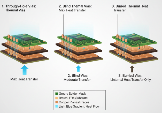
Through-Hole Thermal Vias
These are the most prevalent type of thermal vias, extending completely through the entire thickness of the PCB. They link the top layer to the bottom layer or to internal copper planes, offering an extremely effective direct path for heat to move across multiple layers. Designers frequently arrange through-hole vias in a grid or array directly beneath heat-producing components to maximize thermal transfer efficiency.
Blind Thermal Vias
Blind vias originate on one outer surface of the PCB but terminate within an internal layer, meaning they do not pass entirely through the board. They are useful in designs where an exposed via on the opposite side is undesirable. While generally less effective for overall heat transfer than their through-hole counterparts, blind vias can still contribute to thermal management in specific design contexts.
Buried Thermal Vias
Buried vias are located entirely within the internal layers of a PCB and do not connect to either outer surface. Their primary function is to transfer heat between internal copper planes. However, they are less commonly used for general thermal management strategies because they lack a direct connection to external heat sinks. Their application is usually limited to highly complex, multilayer PCB architectures. For most beginners, through-hole thermal vias remain the most practical and effective choice due to their simplicity and superior heat dissipation capabilities.
What Are the Key Advantages of Incorporating Thermal Vias?
Understanding the "why" behind thermal vias leads us to their tangible benefits. Integrating thermal vias into your PCB layouts offers several significant advantages, particularly for designers aiming to enhance their board's reliability and longevity.
Direct Benefits for PCB Performance
● Enhanced Heat Dissipation: By establishing efficient pathways for heat to escape, thermal vias effectively reduce component temperatures, significantly lowering the risk of damage from overheating.
● Extended Component Life: Maintaining components within their optimal temperature ranges directly contributes to a longer operational lifespan, thereby reducing the need for frequent replacements and associated costs.
● Support for Compact Designs: In an era of shrinking electronic devices, space for large, traditional cooling solutions like bulky heat sinks is often limited. Thermal vias provide effective cooling without consuming valuable board area.
● Cost-Effective Solution: Compared to external cooling mechanisms such as fans or larger heat sinks, implementing thermal vias is an economical approach to managing heat directly within the PCB layout.
● Improved Circuit Stability: Cooler components operate more predictably and efficiently, ensuring the circuit performs consistently without experiencing thermal throttling or instability.
These advantages underscore why thermal vias are an indispensable feature in contemporary PCB designs, especially in high-power or high-density applications where thermal management is paramount.
Best Practices for Designing with Thermal Vias
To maximize the effectiveness of thermal vias in your PCB designs, adherence to specific best practices is essential. These guidelines will help you optimize your thermal management strategy, ensuring your boards perform reliably under varying conditions.
Strategic Placement and Quantity
● Proximity to Heat Sources: Position thermal vias directly beneath or as close as possible to the components that generate the most heat. The shorter the thermal path to the vias, the more efficient the heat transfer. For instance, arranging a 3x3 grid of vias under a power IC can reduce its operating temperature by as much as 15°C in certain scenarios.
● Sufficient Via Count: A single thermal via offers minimal benefit. Employ multiple vias arranged in an array or grid pattern to significantly enhance heat transfer. A general guideline suggests using 8-12 vias per square centimeter under high-power components, though this can vary based on the specific heat load.
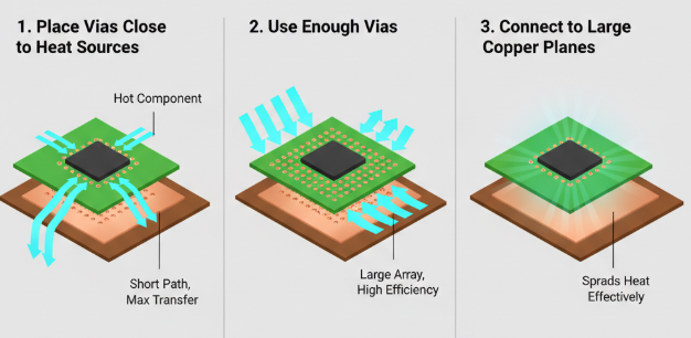
Connection to Copper Planes and Via Filling
● Connection to Large Copper Planes: Thermal vias perform optimally when linked to expansive copper areas, such as ground or power planes, which function as effective heat spreaders. Ensure these planes are as generously sized as possible to facilitate efficient heat dissipation. A ground plane covering 50% of the board's surface, for example, can significantly improve cooling compared to a smaller one.
● Consider Via Filling: For even greater thermal conductivity, consider filling thermal vias with thermally conductive materials like copper or specialized thermal epoxy. Filled vias can boost thermal performance by up to 30% compared to unfilled ones, though this may impact manufacturing costs.
● Avoid Overcrowding: While the inclination might be to add as many vias as possible, excessive numbers can compromise the PCB's structural integrity or interfere with signal routing. Strive for a balance between the number of thermal vias and other critical design requirements, ensuring adequate space for electrical connections.
Common Pitfalls to Avoid When Using Thermal Vias
Even experienced designers can encounter issues when implementing thermal vias. For beginners, being aware of common mistakes can prevent problems and ensure your thermal management strategy is effective.
Key Errors to Prevent
● Incorrect Via Placement: Placing thermal vias too far from the heat source drastically reduces their effectiveness, as heat cannot transfer efficiently.
● Insufficient Via Quantity: A single thermal via or a sparsely arranged group will not provide adequate heat transfer to make a meaningful difference in component temperature.
● Neglecting Copper Plane Connections: Without connecting thermal vias to a sufficiently large copper area, the heat has no effective pathway to dissipate, rendering the vias largely ineffectual.
● Disregarding Manufacturing Constraints: Extremely small vias or overly complex patterns can be challenging and costly to fabricate. Always consult with your large PCB manufacturer regarding their capabilities, including minimum via sizes (typically around 0.3mm diameter).
By avoiding these common errors, you can ensure that your thermal vias function as intended, keeping your PCB cool and stable, even under demanding operational conditions.
Complementary Techniques for Enhanced Heat Management
While thermal vias are a powerful component of any heat dissipation strategy, they are most effective when combined with other thermal management techniques. Integrating multiple methods can significantly improve your PCB's overall thermal performance.
Additional Cooling Strategies
● Heat Sinks: Attaching heat sinks directly to high-power components helps absorb and radiate heat into the surrounding air. Thermal vias can transfer heat from the component to the heat sink, optimizing the cooling effect.
● Copper Pours: Utilizing large areas of copper on the PCB surface helps to spread heat across the board. These "copper pours" work synergistically with thermal vias that connect to internal planes, distributing heat more broadly.
● Thermal Pads: Placing thermal pads beneath components improves the conductive transfer of heat to either the PCB itself or an attached heat sink. These are frequently used in conjunction with vias for maximum thermal efficiency.
● Optimized Component Placement: Thoughtful arrangement of heat-generating components, ensuring adequate spacing between them, can prevent localized hot spots. Distributing heat sources evenly across the board leads to better overall thermal management.
By integrating thermal vias with these complementary methods, designers can create a robust and comprehensive heat dissipation strategy perfectly tailored to the specific needs of their electronic project.
Achieving Superior PCB Designs with Thermal Vias
Thermal vias represent a transformative element for anyone seeking to improve heat dissipation in their PCB designs. By gaining a clear understanding of what thermal vias are, mastering the fundamentals of PCB heat management, identifying various via types for heat transfer, and recognizing their numerous benefits, you are well-equipped to create more reliable and efficient electronic projects. This guide has offered practical advice and best practices, from strategically placing vias to avoiding common design errors.
Whether your project involves a straightforward hobbyist board or a sophisticated multilayer PCB, thermal vias provide an economical and space-efficient solution for maintaining cool component temperatures. Begin incorporating them into your designs today to observe how your projects achieve enhanced performance and prolonged longevity. With a strategic approach, mastering thermal management is well within your grasp!


