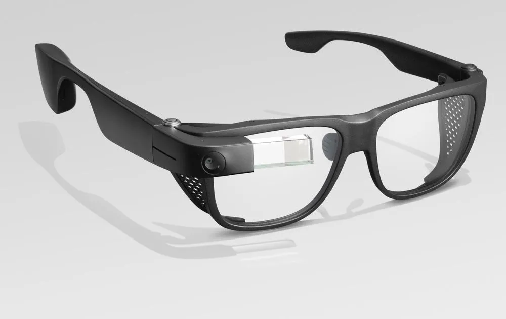
Why Are Flexible PCBs Essential for the Evolution of Smart Eyewear?
Flexible Printed Circuit Boards (FPCs), commonly known as flexible circuits, represent a pivotal advancement in electronics, distinguishing themselves from traditional rigid PCBs by their inherent pliability. Constructed from thin, malleable materials, FPCs can bend, fold, and twist without compromising electrical integrity, making them uniquely suited for compact and curvilinear designs—qualities indispensable for modern smart eyewear. Their capacity to conserve space, significantly reduce weight, and endure numerous bending cycles positions them as the optimal choice for flexible PCB (FPC) applications in wearable technology.
In the highly constrained form factors of smart eyewear, where components must seamlessly integrate into slender frames or conform to the curvature of lenses, flexible PCBs provide the critical interconnectivity required for displays, sensors, batteries, and processors. They facilitate the elegant fusion of advanced technology into a wearable format that prioritizes both user comfort and aesthetic appeal. Without the versatile adaptability of flexible circuits, the sleek, ergonomic designs characteristic of contemporary smart glasses would be virtually unattainable.
Selecting the Optimal Wearable Flexible PCBs Materials for Smart Glasses
The performance, longevity, and overall reliability of flexible PCBs within smart eyewear are fundamentally dependent on the constituent materials. The process of choosing the right flexible PCB materials for smart glasses involves a careful assessment of factors such as inherent flexibility, thermal endurance, and electrical characteristics.
Primary Substrate and Conductive Materials
● Polyimide (PI): This material stands as the most prevalent substrate for flexible PCBs, largely due to its outstanding thermal stability, capable of withstanding temperatures up to 400°C, combined with superior mechanical strength. Polyimide can endure hundreds of thousands of bending cycles, making it an ideal choice for the dynamic and frequently stressed environment of smart eyewear.
● Polyester (PET): Offering a more cost-effective alternative, PET provides good flexibility but is generally less durable and less thermally stable than polyimide. It is often employed in less demanding wearable applications where repeated, high-frequency flexing is not a primary concern.
● Copper Foil: Copper remains the standard conductive material for flexible PCBs. For smart eyewear, rolled annealed (RA) copper is highly preferred over electrodeposited (ED) copper. RA copper exhibits superior flexibility and significantly higher fatigue resistance, which is crucial for circuits that will undergo constant or frequent bending during the lifespan of smart glasses.
Related reading: Embracing Eco-Friendly Electronics: The Rise of Bio-Based Flexible PCBs
Adhesives and Protective Coverlays
● Adhesives: These materials are critical for bonding the various layers of a flexible PCB together. They must maintain their adhesive properties and flexibility even under mechanical stress to prevent delamination.
● Coverlays: These are thin, protective polymer films that encapsulate and shield the exposed circuitry from environmental factors, mechanical abrasion, and electrical shorts. Like adhesives, coverlays must retain their pliability and adhesion to ensure circuit integrity during flexing.
When designing for sophisticated smart eyewear, engineers frequently gravitate towards polyimide-based materials due to their exceptional durability and reliability, particularly in high-end Augmented Reality (AR) glasses. Material selection also significantly influences signal integrity; polyimide, for instance, offers low dielectric loss, making it suitable for high-frequency applications such as 5G connectivity integrated into smart devices.
Key Design Rules for Wearable Flexible PCBs in Smart Eyewear
Designing flexible PCBs for smart eyewear demands strict adherence to specific flex PCB design rules. These guidelines are crucial for ensuring both long-term functionality and structural integrity, as improper design can lead to critical failures such as trace cracking, signal degradation, or catastrophic circuit failure during bending cycles.
Optimizing for Bending Radius and Trace Layout
● Bending Radius for Flexible PCB: This is a paramount design parameter. A tighter bend radius inherently imposes greater mechanical stress on the circuit's copper traces. As a general engineering principle, for dynamic bending (where the PCB experiences continuous, repeated flexing), the minimum bend radius should ideally be at least 10 times the total thickness of the flexible PCB. For static bending (where the PCB is bent once for installation and remains in that position), a minimum bend radius of 3 times the PCB thickness is typically acceptable. For example, a 0.1mm thick flexible PCB would require a minimum dynamic bend radius of 1mm.
● Trace Layout and Spacing: Traces within flexible sections should, whenever possible, be oriented perpendicular to the anticipated bend line. This orientation helps to distribute stress more evenly and minimizes the likelihood of trace fracturing. It is critical to avoid placing vias or discrete components directly within bend areas, as these elements create rigid stress points that are highly susceptible to cracking. Adequate spacing between traces, typically 0.1mm or more, is also essential to prevent inadvertent short circuits that could occur as the circuit flexes.
Related Reading: Constraint Management Techniques for Flexible and Rigid Flex PCBs
Advanced Design Techniques for Reliability
● Tear-Drop Shaped Pads: At the points where traces connect to pads, utilizing tear-drop shaped pads instead of conventional circular pads is highly recommended. This design refinement effectively reduces stress concentration at the critical trace-to-pad junction, significantly mitigating the risk of trace cracking, particularly in high-flex zones within smart eyewear frames.
● Layer Stack-Up Considerations: For multi-layer flexible PCBs, achieving a balanced and symmetrical stack-up is crucial to prevent uneven stress distribution during bending. The "neutral axis"—the plane within the PCB that experiences virtually no tensile or compressive stress during flexing—should ideally be positioned at the geometric center of the board. Symmetrical layer arrangements help to achieve this, which is especially important for smart glasses where the PCB may need to wrap smoothly around curved frame components.
By diligently following these flex PCB design rules, engineers can develop highly reliable circuits capable of enduring the unique and demanding challenges inherent in wearable technology. A well-engineered FPC in smart eyewear, for instance, can reliably withstand over 100,000 bend cycles without any measurable signal degradation, guaranteeing robust long-term performance.
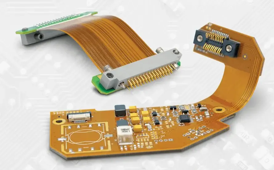
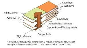
The Rigid-Flex PCB Assembly Process: Combining Adaptability with Stability
Many sophisticated smart eyewear designs leverage rigid-flex PCBs, which ingeniously integrate rigid sections for robust component mounting with flexible sections providing versatile interconnections. The rigid-flex PCB assembly process is inherently more complex than that for purely flexible PCBs but offers unparalleled versatility for highly compact and feature-rich devices.
Step-by-Step Overview of Rigid-Flex Manufacturing
● Material Preparation: The process commences with the meticulous preparation of both rigid and flexible base materials, typically FR4 laminates for the rigid segments and polyimide films for the flexible areas. These diverse materials are then carefully laminated together using specialized adhesive systems formulated to maintain flexibility in the designated bend zones.
● Circuit Patterning: Copper layers are precisely etched to form the intricate circuit patterns on both the rigid and flexible sections. Extreme precision is paramount during this stage to ensure perfect alignment between layers, a critical factor for the high-density interconnects commonly found in smart glasses.
● Drilling and Plating: Holes are precisely drilled for vias (inter-layer connections) and through-hole components. These holes are then plated with copper to establish robust electrical conductivity. Great care must be exercised to prevent any damage to the delicate flexible areas during these mechanical drilling operations.
● Lamination and Bonding: Multiple layers are subsequently laminated together under controlled conditions of heat and pressure. Flexible sections often receive additional coverlays for enhanced protection and insulation, while rigid sections are typically finished with a solder mask layer.
● Component Assembly: Surface-mount technology (SMT) components are precisely placed and soldered onto the rigid sections using automated pick-and-place machines and reflow ovens. Crucially, flexible areas are generally kept free of components to preserve their bendability and prevent stress points.
● Testing and Inspection: The fully assembled rigid-flex PCB undergoes rigorous electrical testing (e.g., flying probe or bed-of-nails) and detailed visual inspection to identify any manufacturing defects, such as open circuits, short circuits, or misaligned layers. For smart eyewear, testing protocols may extend to simulating repeated bending cycles to definitively verify the long-term durability and signal integrity of the flexible sections.
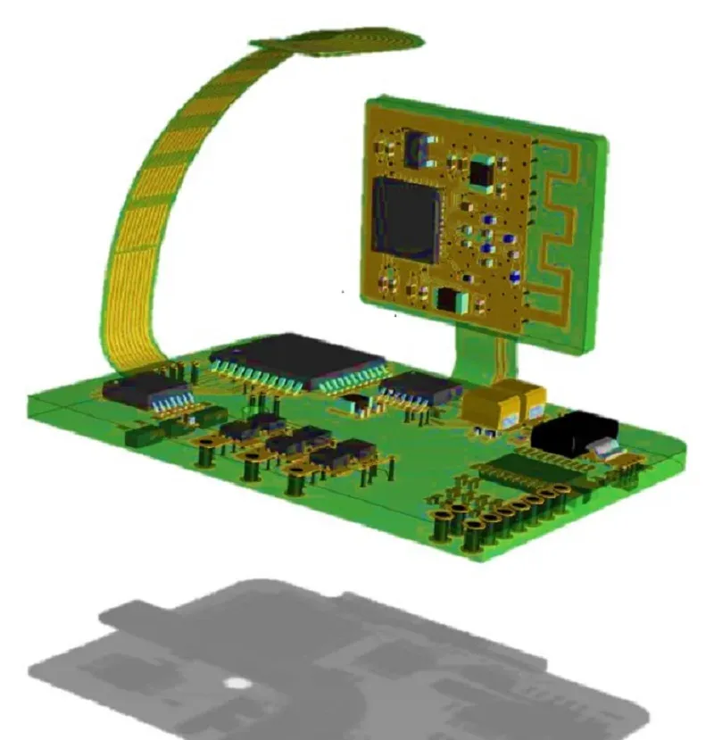
The rigid-flex paradigm is ideally suited for smart eyewear because it enables the stable and secure mounting of critical processors and sensors on the rigid parts, while simultaneously allowing flexible sections to seamlessly connect these components to displays, batteries, or other modules that require movement or precise contouring. This hybrid design significantly reduces the need for bulky connectors and discrete cables, leading to substantial space savings and markedly improving overall system reliability.
Advantages of Flexible PCBs for Wearables in Smart Eyewear Applications
The integration of FPCs into wearable devices, particularly smart eyewear, offers a multitude of advantages that directly address the inherent challenges of designing compact, ergonomic, and user-friendly technology. These benefits are pivotal for enabling the next generation of smart wearables.
Space, Weight, and Durability Benefits
● Exceptional Space Efficiency: FPCs can be ingeniously folded, twisted, or shaped to conform precisely to the tight and often irregular volumetric constraints within devices, such as the slender arms or intricate contours of smart glasses. This adaptability dramatically reduces the overall physical footprint of the electronic device.
● Significant Weight Reduction: Weighing considerably less than their rigid PCB counterparts, FPCs contribute substantially to the lightweight design essential for comfortable, all-day wear in smart eyewear, a critical factor for user acceptance.
● Enhanced Durability: High-quality FPCs are engineered to withstand repeated and dynamic flexing without experiencing electrical or mechanical failure. This ensures that smart glasses remain fully functional and reliable over an extended period of extensive daily use.
● Minimized Interconnects: By integrating multiple connection pathways directly into a single flexible substrate, FPCs largely eliminate the need for bulky discrete connectors, cumbersome wire harnesses, and separate cables. This simplification streamlines the assembly process, reduces potential points of failure, and significantly enhances overall system reliability, which is paramount for maintaining signal integrity, especially in high-frequency applications.
For instance, within the sophisticated architecture of AR glasses, an FPC can fluidly connect a miniature display embedded within the lens area to a primary control unit housed in the frame, gracefully bending around optical components and structural corners without adding any perceptible bulk. This level of seamless integration is precisely why FPCs have become an indispensable cornerstone of modern wearable technology.
Challenges and Advanced Solutions in Wearable Flexible PCB Manufacturing for Smart Eyewear
Manufacturing flexible PCBs for smart eyewear presents a unique set of technical challenges, primarily due to the devices' miniaturization, dynamic usage, and high-performance requirements. However, continuous advancements in materials science and fabrication technologies have yielded effective solutions.
Overcoming Key Manufacturing Hurdles
● Challenge: Maintaining Signal Integrity at High Frequencies: High-frequency signals, such as those crucial for wireless communication (e.g., Wi-Fi, Bluetooth, 5G) in smart eyewear, can suffer degradation due to the typically thin dielectric layers and potential variations in material properties within flexible PCBs.
○ Solution: Manufacturers address this by utilizing specialized low-loss flexible materials, such as modified polyimide variants, and implementing extremely precise impedance control techniques. This involves meticulously designing trace widths and dielectric layer thicknesses to achieve target impedance values (e.g., 50 ohms for single-ended lines), ensuring optimal signal transmission with minimal attenuation and reflection.
● Challenge: Ensuring Long-Term Bend Durability: The frequent and repeated bending cycles inherent in smart eyewear usage can induce fatigue in copper traces, leading to eventual cracking and circuit failure.
○ Solution: To counteract this, manufacturers employ advanced materials like rolled annealed (RA) copper foil, which exhibits superior ductility and fatigue resistance compared to standard electrodeposited copper. Additionally, strategic reinforcement of critical bend areas with stiffeners (e.g., polyimide or FR4 overlays) or extra coverlay layers helps to distribute mechanical stress more evenly, significantly extending the circuit's operational life.
● Challenge: Extreme Miniaturization and High-Density Interconnects (HDI): Smart eyewear demands incredibly compact PCBs with exceptionally high-density interconnects to pack complex functionality into minimal space.
○ Solution: This challenge is met through the application of advanced manufacturing techniques, such as laser drilling for creating microvias (with diameters as small as 0.05mm), fine-line etching processes for incredibly narrow traces, and sophisticated layer-to-layer registration systems. These processes enable the creation of highly compact, multi-layer flexible circuits capable of delivering the required performance in a tiny footprint.
Related Reading: Flexible PCB Design for Wearable Health Tech: An Advanced Guide
Conclusion: Wearable Flexible PCBs — Powering the Next Generation of Smart Eyewear
Flexible Printed Circuit Boards are undeniably the foundational technology underpinning smart eyewear, enabling the sleek, lightweight, and functionally rich designs that today’s discerning users expect. From the initial selection of the most suitable flexible PCB materials for smart glasses to the meticulous application of flex PCB design rules, and from precisely calculating the bending radius for flexible PCBs to flawlessly executing the rigid-flex PCB assembly process, every single step is critically important for the ultimate success of these innovative devices. Understanding these integral elements empowers designers and manufacturers to create highly reliable and truly groundbreaking products.
At AIVON, we are deeply committed to empowering engineers and manufacturers in their pursuit of crafting cutting-edge solutions for smart eyewear and beyond. With our extensive expertise in the production of both flexible and rigid-flex PCBs, we furnish the essential tools, resources, and technical guidance necessary to transform your visionary designs into tangible, high-performance realities. We invite you to delve into the dynamic world of flexible circuits and discover firsthand how their unparalleled adaptability and robust performance can fundamentally transform your forthcoming wearable technology project.


