Introduction
Electric vehicle charging stations are pivotal in the transition to sustainable transportation. These systems demand robust and reliable components to handle high power levels, ensure safety, and maintain efficiency. Among these components, printed circuit boards play a critical role, especially when designed with heavy copper layers. Heavy copper PCBs are uniquely suited for the intense current and thermal demands of electric vehicle charging infrastructure. This article explores the essential design considerations for integrating heavy copper PCBs into charging stations. Key focus areas include thermal management, high voltage safety, and overall PCB design principles. By addressing these factors, engineers can create systems that meet the rigorous requirements of modern electric vehicle charging applications, ensuring durability and performance under challenging conditions.
What Are Heavy Copper PCBs and Why Do They Matter?
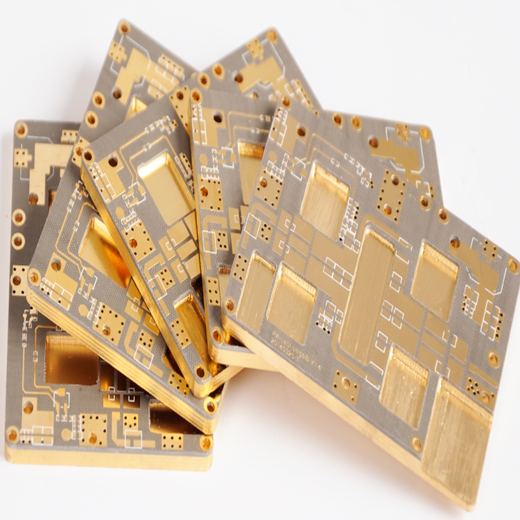
Heavy copper PCBs are defined by their thicker copper layers, typically exceeding 3 ounces per square foot, compared to standard PCBs with 1 to 2 ounces. This increased copper thickness enhances current carrying capacity and improves heat dissipation, making them ideal for high power applications like electric vehicle charging stations. In such systems, where power levels can reach several kilowatts, managing electrical and thermal stress is paramount. Heavy copper PCBs mitigate risks of overheating and voltage breakdown, directly impacting reliability and safety. Their ability to withstand harsh operating environments also extends the lifespan of charging equipment. For engineers, selecting heavy copper PCBs ensures compliance with industry demands for efficiency and durability in electric vehicle charging infrastructure.
Related Reading: Heavy Copper PCB: An overview of its benefits and applications
Technical Principles of Heavy Copper PCBs in Charging Stations
Current Handling Capabilities
Heavy copper PCBs excel in managing high current loads, a fundamental requirement for electric vehicle charging stations. Thicker copper traces reduce electrical resistance, allowing the board to carry substantial current without significant voltage drop or power loss. This is critical for fast charging systems, where currents can exceed 100 amperes. By minimizing resistance, these PCBs prevent excessive heat generation, a common failure point in high power electronics. Engineers must calculate trace width and thickness based on current requirements to avoid bottlenecks, ensuring consistent performance during peak operation.
Thermal Dissipation Mechanisms
Thermal management is a core concern in PCB design for charging stations. Heavy copper layers act as effective heat sinks, distributing thermal energy across the board and away from critical components. This reduces the risk of thermal runaway, where excessive heat damages components or degrades performance. The larger copper mass absorbs and dissipates heat more efficiently than standard boards, maintaining operational stability. Incorporating thermal vias and ensuring adequate copper coverage are essential strategies to enhance heat transfer, protecting the system under continuous high power operation.
High Voltage Insulation and Safety
Electric vehicle charging stations often operate at voltages exceeding 400 volts, posing significant safety risks if not managed properly. Heavy copper PCBs must be designed with sufficient insulation to prevent arcing or breakdown between traces. Adhering to industry standards, such as those outlined in IEC 60950-1 for information technology equipment safety, ensures proper creepage and clearance distances. These distances are critical to avoid electrical discharge in high voltage environments. Engineers must also select dielectric materials with high breakdown strength to maintain insulation integrity under stress.
Practical Design Considerations for Heavy Copper PCBs
Material Selection for Durability
Choosing the right substrate and dielectric materials is vital for heavy copper PCB performance in charging stations. High thermal conductivity materials, such as those meeting IPC-4101 specifications for laminate materials, support effective heat dissipation. The substrate must also withstand mechanical stress and environmental factors like humidity and temperature fluctuations common in outdoor charging installations. Engineers should prioritize materials with low thermal expansion coefficients to minimize warpage or delamination during operation, ensuring long term reliability.
Trace Width and Spacing for High Current
Designing trace width and spacing is a balancing act between current capacity and board size. Wider traces accommodate higher currents but increase board dimensions, while narrow traces risk overheating. Standards like IPC-2221 for generic PCB design provide guidelines for calculating minimum trace widths based on current and temperature rise. For high voltage safety, spacing between traces must prevent arcing, adhering to clearance requirements specified in relevant standards. Precise calculations and simulations are necessary to optimize layouts for electric vehicle charging applications.
Thermal Management Strategies
Effective thermal management extends beyond copper thickness. Incorporating thermal vias, which are small holes filled with conductive material, enhances heat transfer from hot spots to outer layers or heat sinks. Placing these vias near high power components maximizes their impact. Additionally, ensuring uniform copper distribution across layers prevents localized overheating. Engineers can also integrate external cooling solutions, such as fans or heat pipes, to complement the PCB's inherent thermal capabilities. These strategies collectively maintain safe operating temperatures.
High Voltage Safety Measures
Safety in high voltage environments requires meticulous attention to PCB layout. Creepage and clearance distances must comply with standards like IEC 60664-1 for insulation coordination. These distances depend on the operating voltage, pollution degree, and material properties. Using conformal coatings or potting compounds adds an extra layer of protection against environmental contaminants that could compromise insulation. Regular testing for dielectric strength and insulation resistance, as per IPC-TM-650 test methods, validates the design's safety under real world conditions.
Layer Stackup and Signal Integrity
The layer stackup in heavy copper PCBs must balance power distribution and signal integrity. Thicker copper layers can introduce parasitic capacitance and inductance, affecting high frequency signals in control circuits. Engineers should segregate power and signal layers, using ground planes to shield sensitive traces from interference. Standards like IPC-6012 for rigid PCB performance provide guidance on layer thickness and impedance control. A well planned stackup ensures reliable operation of both power delivery and communication functions in charging stations.
Related Reading: Heavy Copper Handling: Designing PCBs for High-Power Industrial Applications
Troubleshooting Common Issues in Heavy Copper PCB Design
Heavy copper PCBs, while robust, can present unique challenges during design and operation. One common issue is uneven heat distribution, leading to hot spots near high current components. This can be mitigated by redistributing copper or adding thermal vias strategically. Another concern is mechanical stress during manufacturing, as thicker copper increases board rigidity, potentially causing cracking. Adhering to IPC-A-600 for acceptability of printed boards helps identify and address such defects early. High voltage designs may also exhibit partial discharge if creepage distances are inadequate. Routine testing and layout adjustments resolve this risk. Engineers must remain vigilant during prototyping to catch and correct these issues before full scale production.
Conclusion
Heavy copper PCBs are indispensable for the reliable operation of electric vehicle charging stations. Their ability to handle high currents, manage thermal loads, and ensure safety under high voltage conditions makes them a cornerstone of modern charging infrastructure. By focusing on critical design considerations like material selection, trace layout, thermal management, and insulation, engineers can optimize these boards for peak performance. Adherence to established industry standards guarantees that designs meet safety and reliability expectations. As the demand for efficient electric vehicle charging grows, leveraging the strengths of heavy copper PCBs will be essential for sustainable and safe solutions in this evolving field.
FAQs
Q1: How do heavy copper PCBs improve thermal management in electric vehicle charging stations?
A1: Heavy copper PCBs enhance thermal management by utilizing thicker copper layers to dissipate heat efficiently. Their increased thermal mass absorbs and spreads heat away from critical components, reducing the risk of overheating during high power operation. Incorporating thermal vias further aids in transferring heat to outer layers. This approach ensures stable performance and extends the lifespan of charging equipment under continuous load.
Q2: What safety standards apply to high voltage PCB design for charging stations?
A2: High voltage PCB design for electric vehicle charging must comply with standards like IEC 60664-1 for insulation coordination and IEC 60950-1 for safety requirements. These standards define creepage and clearance distances to prevent arcing. Regular testing, as outlined in IPC-TM-650, validates insulation integrity. Following these guidelines ensures safe operation in environments exceeding 400 volts, protecting both equipment and users.
Q3: Why is trace width critical in heavy copper PCB design for electric vehicle charging?
A3: Trace width in heavy copper PCBs directly impacts current carrying capacity and heat generation. Wider traces handle higher currents without excessive temperature rise, crucial for fast charging systems. Standards like IPC-2221 provide calculation methods to determine minimum widths based on current load. Proper design prevents overheating and ensures reliable power delivery in electric vehicle charging applications.
Q4: How does material selection affect heavy copper PCB performance in high voltage environments?
A4: Material selection significantly influences heavy copper PCB performance in high voltage settings. Substrates meeting IPC-4101 specifications offer high thermal conductivity and low expansion, reducing warpage. Dielectric materials with high breakdown strength maintain insulation under stress. Choosing appropriate materials ensures durability, safety, and efficiency in electric vehicle charging stations exposed to harsh conditions.
References
IPC-2221B — Generic Standard on Printed Board Design. IPC, 2012.
IPC-6012E — Qualification and Performance Specification for Rigid Printed Boards. IPC, 2020.
IPC-A-600K — Acceptability of Printed Boards. IPC, 2020.
IPC-4101E — Specification for Base Materials for Rigid and Multilayer Printed Boards. IPC, 2017.
IPC-TM-650 — Test Methods Manual. IPC, 2021.
IEC 60664-1:2021 — Insulation Coordination for Equipment within Low-Voltage Systems. IEC, 2021.
IEC 60950-1:2005+AMD1:2009+AMD2:2013 — Information Technology Equipment - Safety. IEC, 2013.


