Introduction
High-frequency PCB design presents unique challenges where signal integrity becomes paramount. As operating frequencies exceed 1 GHz and signal rise times drop below 1 ns, even minor impedance discontinuities can cause signal reflections that degrade performance. These reflections lead to issues like overshoot, ringing, and crosstalk, ultimately compromising data rates and system reliability. Buried resistors offer a precise solution for impedance matching by embedding termination resistors directly within the PCB layers, eliminating surface-mount components that introduce parasitics. This approach enhances buried resistors impedance control, supporting high-frequency PCB design requirements for applications such as telecommunications, computing, and radar systems. By integrating buried resistors, designers achieve better signal reflections management and overall impedance matching without sacrificing board real estate.
Engineers must prioritize controlled impedance traces alongside strategic resistor placement to maintain signal integrity. Traditional surface termination resistors add inductance and capacitance, exacerbating reflections in high-speed environments. Buried resistors, positioned closer to the signal path, provide low-inductance termination that aligns with transmission line theory. This method aligns with industry needs for compact, high-performance boards. The following sections explore the principles, implementation, and best practices for leveraging buried resistor signal integrity in modern designs.
What Are Buried Resistors and Why Do They Matter for Impedance Control?
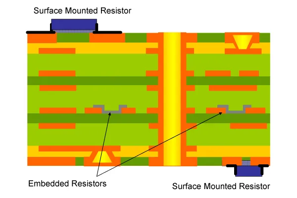
Buried resistors are passive components embedded within the internal layers of a multilayer PCB, typically fabricated using resistive foils, polymer thick films, or thin-film materials integrated during lamination. Unlike discrete surface-mount resistors, these are patterned through etching processes to achieve specific resistance values based on length-to-width ratios. This embedding process allows resistors to connect directly to inner-layer traces, minimizing parasitic effects that plague high-frequency signals. In high-frequency PCB design, buried resistors enable precise termination at the end of transmission lines, ensuring characteristic impedance remains consistent.
The primary advantage lies in their contribution to buried resistors impedance control by reducing loop inductance and surface area disruptions. Surface components often create stubs that reflect signals, but buried variants sit flush within the stackup, promoting smoother current return paths. This is crucial for maintaining signal reflections below acceptable thresholds in dense layouts. Additionally, they free up top-layer space for routing critical high-speed nets, optimizing board density without compromising performance.
Industry standards like IPC-2221 address the design of such embedded passives, providing guidelines for material selection and layout to ensure reliability. Engineers value buried resistors for their thermal stability and reduced sensitivity to mechanical stress compared to discrete parts. As board complexity increases, these resistors become essential for achieving target impedances in stripline or microstrip configurations. Their role in impedance matching extends to series, parallel, or Thevenin terminations, tailored to specific signal requirements.
Understanding Signal Reflections in High-Frequency PCB Design
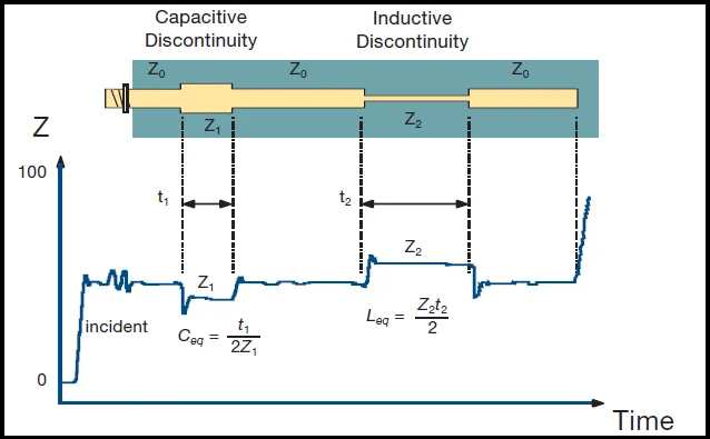
Signal reflections occur when a voltage wave encounters an impedance discontinuity along a transmission line, partially bouncing back toward the source. In PCB traces, the characteristic impedance Z0 depends on trace geometry, dielectric constant, and layer stackup. Mismatches arise from unterminated lines, vias, or bends, quantified by the reflection coefficient Γ = (Z_L - Z0) / (Z_L + Z0), where Z_L is the load impedance. For high-frequency PCB design, even a 10% deviation can introduce unacceptable ringing, distorting eye diagrams and increasing bit error rates.
Transmission line theory dictates that signals propagate as TEM waves in controlled impedance environments, but reflections disrupt this balance. Fast rise times amplify the issue, as wavelength shortens relative to trace length; a 100 ps edge corresponds to frequencies up to 10 GHz. Common culprits include open stubs, impedance steps at connectors, and capacitive loading from nearby components. Time-domain reflectometry (TDR) measurements reveal these discontinuities as impedance spikes or dips on the trace waveform.
Crosstalk between adjacent traces worsens with poor impedance control, coupling energy via mutual inductance or capacitance. In multilayer boards, reference planes must provide continuous return paths to minimize loop area. High-frequency effects like skin effect further narrow effective conductor width, altering Z0. Engineers simulate these behaviors early to predict and mitigate reflections, ensuring compliance with signal integrity budgets.
Technical Principles of Buried Resistors for Impedance Matching
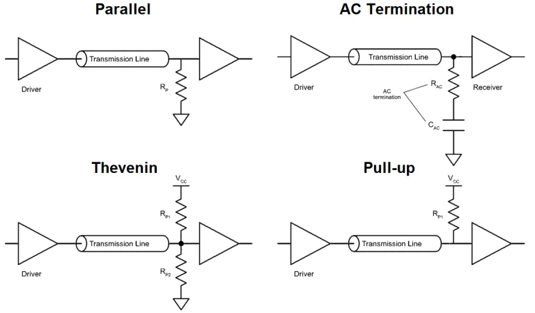
Buried resistors function as termination elements by absorbing incident waves, preventing reflections through matched loading. In a parallel termination scheme, the resistor value equals Z0, shunting excess energy to ground via the nearest plane. Series termination places the resistor near the driver, matching source output impedance to line Z0 and eliminating initial reflections. Thevenin equivalents combine both for bidirectional lines, calculated as R_th = 2 * Z0 for 50-ohm systems.
Fabrication involves laminating a resistive layer between dielectrics, then photoresist etching to define resistor patterns. Resistance R = ρ * (L / W * t), where ρ is sheet resistivity, L length, W width, and t thickness. Tolerances typically range from 5% to 10%, influenced by etching precision and material uniformity. In high-frequency contexts, low-inductance placement reduces ESL, preserving wideband performance up to multi-GHz ranges.
IPC-2141 provides equations for calculating Z0 in microstrip and stripline geometries, essential for aligning buried resistor values with trace impedances. Dielectric materials with low loss tangent (tan δ < 0.005) minimize attenuation alongside reflections. Temperature coefficients of resistive materials must match the stackup to avoid drift under thermal cycling. This integration ensures buried resistor signal integrity across operating conditions.
Power handling limits resistor size, balancing thermal dissipation with board constraints. Simulations verify eye opening and jitter with buried elements, confirming reflection coefficients below -20 dB.
Best Practices for Implementing Buried Resistors in High-Frequency PCBs
Start with stackup optimization, positioning buried resistors on inner layers adjacent to signal planes for shortest return paths. Select materials with stable dielectric constants (Dk 3.0-4.5) and controlled thickness tolerances (<10%). Trace widths for 50-ohm single-ended or 100-ohm differential pairs follow IPC-2141 formulas, iterated with fab capabilities. Simulate full channel including resistors to predict insertion loss and return loss.
Manufacturing requires tight process controls: laser trimming post-etch for tolerance adjustment, though pre-etch design dominates. Specify sheet rho and TCR in fab drawings, verifying via test coupons. Layer sequencing places resistors away from high-current planes to avoid heating. Vias connecting to buried resistors demand back-drilling to remove stubs, preserving impedance matching.
Testing protocols include TDR for Z0 verification and VNA for S-parameters, targeting VSWR <1.2. Qualification per IPC-6012 ensures performance under thermal, mechanical, and humidity stress. Collaborate with fabricators on DFM reviews to address yield factors like alignment registration. These practices solidify buried resistors impedance control in production.
Troubleshooting Common Issues in Buried Resistor Signal Integrity
Tolerance variations from etching non-uniformity manifest as inconsistent termination, visible as elevated reflections on TDR. Calibrate processes with statistical process control on coupons. Thermal drift shifts resistance, addressed by selecting low-TCR materials and modeling junction temperatures.
Process-induced defects like delamination at resistive-dielectric interfaces cause opens; inspect via cross-sectioning. Excessive power density leads to hotspots, mitigated by derating and plane proximity for heat spreading. Signal probing disturbs buried setups, so rely on non-contact methods like near-field scanning.
Conclusion
Buried resistors revolutionize high-frequency PCB design by providing embedded impedance matching that tames signal reflections effectively. Their integration minimizes parasitics, optimizes space, and upholds signal integrity essential for modern electronics. Adhering to structured design principles and standards ensures reliable performance. Engineers can confidently deploy this technology for superior outcomes in demanding applications.
FAQs
Q1: What role do buried resistors play in high-frequency PCB design for impedance control?
A1: Buried resistors terminate transmission lines internally, matching characteristic impedance to prevent signal reflections. They reduce inductance compared to surface parts, supporting rise times under 100 ps. This enhances buried resistors impedance control, crucial for maintaining eye diagrams in GHz-range signals. Design per stackup geometry ensures precision.
Q2: How do signal reflections impact impedance matching in PCBs?
A2: Reflections from mismatches cause ringing and jitter, degrading signal integrity. Proper impedance matching absorbs waves, with buried resistors providing low-parasitic termination. In high-frequency PCB design, TDR confirms discontinuities below 5%. This alignment minimizes crosstalk and supports higher data rates.
Q3: What are best practices for buried resistor signal integrity?
A3: Optimize stackup for short return paths, select low-loss dielectrics, and verify with TDR/VNA. Control tolerances via etching and trimming, avoiding thermal hotspots. IPC standards guide layout for reliability. These steps ensure consistent performance in production.
Q4: Can buried resistors handle multi-GHz frequencies effectively?
A4: Yes, their embedded nature minimizes ESL, preserving wideband matching. Material choices with low tan δ support frequencies beyond 5 GHz. Simulations predict behavior, confirming low return loss. This makes them ideal for buried resistor signal integrity in RF applications.
References
IPC-2141A — Design Guide for High-Speed Controlled Impedance Circuit Boards. IPC.
IPC-2221B — Generic Standard on Printed Board Design. IPC.
IPC-6012E — Qualification and Performance Specification for Rigid Printed Boards. IPC, 2017