Introduction
Impedance control is a cornerstone of modern printed circuit board (PCB) design, particularly in high-speed applications like telecommunications. As signal frequencies increase, maintaining signal integrity along the communication path becomes critical to prevent issues such as signal attenuation and reflections. Power plane design plays a vital role in achieving the right termination for transmission lines, helping to reduce the effects of noise and electromagnetic interference. This article explores the principles of impedance control, the significance of power plane configurations, and practical strategies for optimizing PCB layouts. Aimed at electrical engineers, the discussion will focus on technical mechanisms and actionable design practices to ensure robust performance in telecommunication systems where reliable data transmission is paramount.
What Is Impedance Control and Why It Matters
Impedance control refers to the deliberate management of the characteristic impedance of transmission lines on a PCB to match the source and load impedances. In telecommunications, where high-frequency signals are common, mismatched impedance can lead to signal reflections, causing data loss or corruption along the communication path. Proper impedance control minimizes signal attenuation, ensuring that signals reach their destination with minimal degradation.
The importance of impedance control extends beyond signal integrity. It directly impacts power delivery and noise reduction, both of which are critical in high-speed designs. A well-designed power plane supports impedance control by providing a low-impedance return path for signals, reducing the effects of crosstalk and electromagnetic interference. For engineers working on telecommunication systems, understanding and implementing impedance control is essential to meet stringent performance requirements and maintain reliable operation under demanding conditions.
Technical Principles of Impedance Control with Power Planes
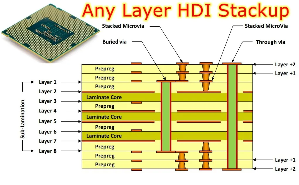
Impedance in a PCB is influenced by several factors, including trace geometry, dielectric material properties, and the proximity of reference planes. The characteristic impedance of a transmission line is determined by its inductance and capacitance per unit length. In high-frequency designs common in telecommunications, microstrip and stripline configurations are often used, each requiring precise control to achieve the desired impedance.
Power planes serve as reference planes in PCB stackups, offering a stable ground or power return path. Their design significantly affects impedance by altering the capacitance between the signal trace and the reference plane. A continuous, unbroken power plane reduces loop inductance, providing a low-impedance path that helps to minimize signal attenuation. Conversely, splits or discontinuities in the plane can introduce impedance mismatches, leading to reflections and noise.
The dielectric constant of the substrate material also plays a role in impedance control. Materials with consistent dielectric properties ensure uniform impedance across the board, which is vital for maintaining signal integrity in the communication path. Engineers must account for these factors during the design phase to achieve the right termination for high-speed signals, preventing issues like overshoot or ringing that degrade performance.
Related Reading: PCB stackup affects impedance control
Role of Power Planes in Reducing Signal Attenuation
Power planes are not just for power distribution; they are integral to signal integrity in high-speed designs. By acting as a reference for signal traces, power planes help maintain consistent impedance, which is crucial in telecommunications where signal attenuation must be minimized. A solid power plane reduces the loop area for return currents, lowering inductance and thereby decreasing noise coupling between adjacent traces.
Inadequate power plane design, such as excessive cuts or slots, can disrupt the return path, increasing impedance and causing signal reflections. This is particularly problematic in high-frequency applications where even minor disruptions can lead to significant signal loss. To reduce the effects of such issues, engineers must ensure that power planes are as continuous as possible, with minimal interruptions, to support a stable communication path.
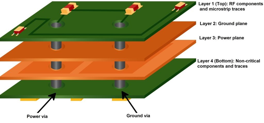
Additionally, the placement of power planes in the PCB stackup influences impedance control. Positioning a power plane adjacent to a signal layer in a multilayer board enhances capacitive coupling, stabilizing impedance. This approach is especially effective in reducing signal attenuation for high-speed signals, ensuring that data transmission remains reliable across long traces.

Practical Solutions for Impedance Control in Power Plane Design
Achieving effective impedance control with power plane design requires a systematic approach. Below are key strategies that electrical engineers can apply to optimize PCB layouts for telecommunications applications.
- Optimize Stackup Configuration: Design the PCB stackup to include dedicated power and ground planes adjacent to signal layers. This arrangement ensures a low-impedance return path, reducing the effects of noise and signal attenuation. A typical four-layer stackup might include signal layers on the top and bottom, with internal power and ground planes.
- Minimize Plane Discontinuities: Avoid unnecessary splits or cuts in power planes, as these can disrupt return currents and cause impedance mismatches. If splits are unavoidable, ensure that signal traces do not cross them to maintain the right termination and protect the communication path.
- Control Trace Geometry: Adjust the width and spacing of signal traces to achieve the target impedance. Wider traces lower impedance, while narrower traces increase it. Use impedance calculators based on industry-standard formulas to determine appropriate dimensions for specific dielectric materials.
- Select Appropriate Materials: Choose substrate materials with stable dielectric constants and low loss tangents to minimize signal attenuation. Consistency in material properties across the board prevents variations in impedance, which is critical for high-frequency signals in telecommunications.
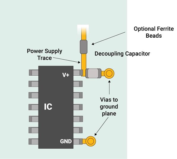
- Implement Decoupling Capacitors: Place decoupling capacitors near power pins of active components to stabilize voltage levels on the power plane. This reduces noise and supports impedance control by filtering high-frequency transients that could affect signal integrity.
Related Reading: Power Plane Decoupling: A Comprehensive Guide to PCB Stability
Best Practices for High-Speed Telecommunication Designs
In telecommunication systems, where high data rates are standard, impedance control becomes even more critical. Engineers must focus on maintaining a robust communication path to handle gigabit-speed signals without degradation. One best practice is to route high-speed signals on layers adjacent to a continuous ground or power plane. This minimizes the loop area for return currents, reducing electromagnetic interference.
Another important consideration is the right termination of transmission lines. Termination techniques, such as series or parallel resistors, can be used to match the impedance of the source and load, preventing reflections that contribute to signal attenuation. Proper termination ensures that signals propagate efficiently along the communication path, maintaining data integrity.
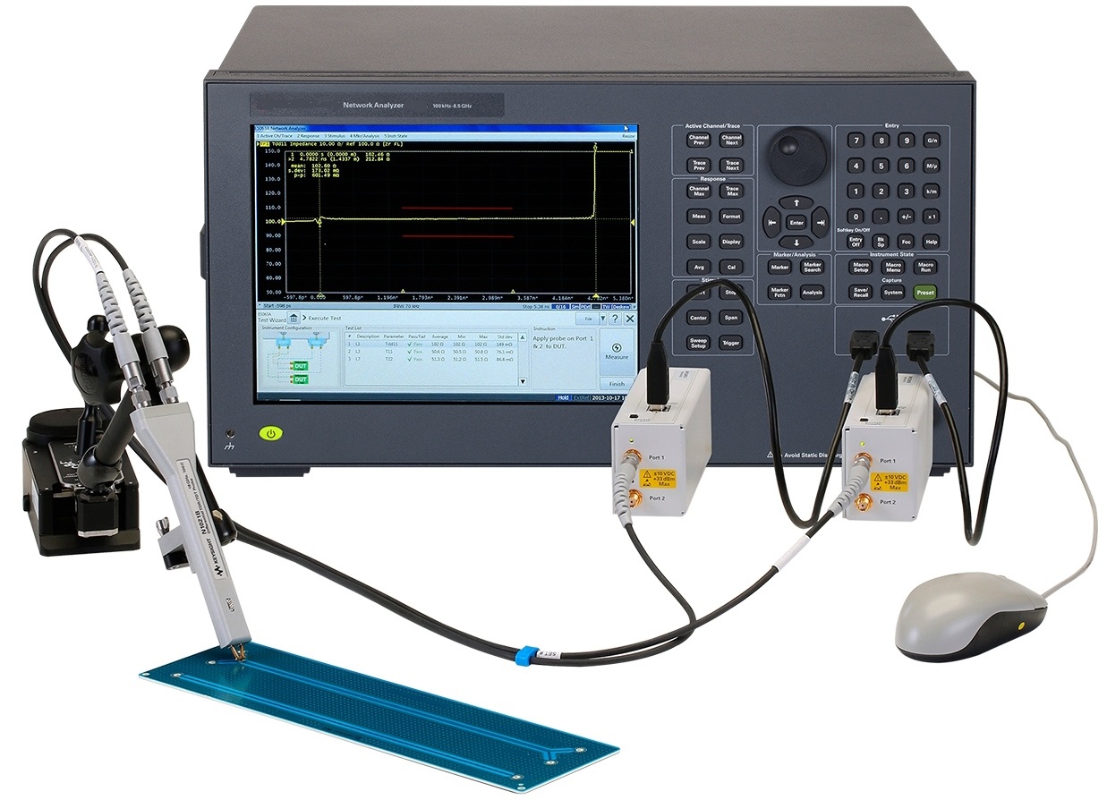
Regular simulation and testing during the design phase are also recommended. Tools that model electromagnetic fields can predict impedance variations and highlight potential issues in power plane design. By validating the layout before fabrication, engineers can reduce the effects of mismatches and optimize performance for telecommunication applications.
Challenges in Impedance Control and Mitigation Strategies
Designing for impedance control with power planes is not without challenges. One common issue is the variation in dielectric properties across different batches of PCB materials. Such inconsistencies can lead to unexpected impedance shifts, affecting signal integrity. To mitigate this, engineers should specify materials that comply with recognized standards and verify their properties during incoming inspection.
Another challenge is managing thermal effects in high-power telecommunication systems. Temperature changes can alter the dielectric constant of materials, impacting impedance. Designing with adequate thermal reliefs and ensuring proper heat dissipation can help maintain consistent performance under varying conditions.
Finally, manufacturing tolerances can introduce deviations in trace widths or layer thicknesses, affecting impedance. Collaborating with fabricators to adhere to tight tolerances, as outlined in industry standards like IPC-6012E, ensures that the final board matches the design intent, preserving the communication path integrity.
Conclusion
Impedance control with power plane design is a fundamental aspect of PCB engineering, especially in telecommunications where high-speed signals demand precise management of the communication path. By understanding the technical principles behind impedance, optimizing power plane configurations, and applying best practices, engineers can significantly reduce the effects of signal attenuation and noise. Practical solutions, such as careful stackup design and proper termination, ensure reliable performance in demanding applications. As frequencies continue to rise, mastering these techniques will remain essential for maintaining signal integrity and achieving robust system designs.
FAQs
Q1: How does power plane design impact signal attenuation in telecommunications?
A1: Power plane design directly affects signal attenuation by providing a low-impedance return path for high-speed signals in telecommunications. A continuous plane minimizes loop inductance, reducing noise and reflections that degrade signal strength. Proper placement near signal layers enhances capacitive coupling, stabilizing impedance and ensuring efficient data transmission along the communication path.
Q2: What is the right termination for high-speed signals in PCB design?
A2: The right termination for high-speed signals involves matching the impedance of the source and load to prevent reflections. Techniques like series or parallel termination using resistors can be applied. This ensures minimal signal loss and maintains integrity across the communication path, which is critical for high-frequency applications in modern systems.
Q3: How can engineers reduce the effects of impedance mismatches in PCBs?
A3: Engineers can reduce the effects of impedance mismatches by optimizing trace geometry, using consistent dielectric materials, and ensuring continuous power planes. Simulation tools help predict and address variations. Adhering to tight manufacturing tolerances and validating designs against standards also minimizes mismatches, protecting signal quality in critical applications.
Q4: Why is the communication path critical in high-speed PCB designs?
A4: The communication path is vital in high-speed PCB designs as it determines how effectively signals travel without degradation. Proper impedance control and power plane design prevent issues like signal attenuation and reflections. A well-designed path ensures reliable data transfer, which is essential for performance in telecommunications and other high-frequency systems.
References
IPC-6012E - Qualification and Performance Specification for Rigid Printed Boards. IPC, 2020.
IPC-A-600K - Acceptability of Printed Boards. IPC, 2020.
IPC-2141A - Design Guide for High-Speed Controlled Impedance Circuit Boards. IPC, 2004.