Introduction
Radio Frequency (RF) PCB design demands precision to ensure optimal performance in high-frequency applications. Vias, as critical interconnects between layers, play a significant role in maintaining signal integrity and minimizing parasitic effects like inductance. Poorly designed vias can introduce noise, signal loss, and electromagnetic interference, compromising the entire circuit. This article explores RF PCB via design rules, focusing on strategies to reduce inductance and enhance signal quality. Key considerations include RF PCB via placement, stitching techniques, and the use of blind and buried vias. Written for electrical engineers, this guide provides technical insights and practical solutions aligned with industry standards to help designers achieve reliable RF performance in complex layouts.
What Are RF PCB Vias and Why Do They Matter?
Vias are conductive pathways that connect different layers of a printed circuit board. In RF PCB design, vias are essential for routing high-frequency signals between layers while maintaining impedance control. However, vias introduce parasitic inductance and capacitance, which can distort signals and degrade performance at high frequencies. RF PCB via inductance becomes a critical concern as it can cause signal delays and reflections, especially in applications like wireless communication, radar systems, and microwave circuits.
The importance of proper via design lies in its impact on signal integrity. A well-designed via minimizes electromagnetic interference and ensures consistent impedance along the signal path. For RF engineers, understanding how to optimize via structures is vital to achieving low-loss transmission and reliable operation in high-speed circuits. This directly affects the efficiency and functionality of the final product.
Technical Principles of RF PCB Via Inductance
At high frequencies, vias behave as inductors due to their physical structure. The inductance of a via depends on its length, diameter, and proximity to ground planes. Longer vias have higher inductance because the current path through the via barrel increases. Similarly, narrower vias exhibit higher inductance due to reduced cross-sectional area for current flow. This parasitic effect can create impedance mismatches, leading to signal reflections and power loss.
Another factor is the via's interaction with surrounding conductive layers. Without proper grounding, vias can act as unintended antennas, radiating electromagnetic energy and causing interference. The loop area formed by the signal via and its return path also contributes to inductance. A larger loop area results in higher inductance, amplifying signal distortion. Understanding these principles helps engineers design vias that minimize such effects in RF applications.
Related Reading: Microvia PCB for RF Applications: Design Considerations for High Frequency Performance
RF PCB Via Design Rules for Optimal Performance
Designing vias for RF PCBs requires adherence to specific guidelines to reduce inductance and preserve signal integrity. Below are key RF PCB via design rules based on widely accepted industry practices.
Minimize Via Length and Diameter
Shorter vias reduce the inductive path, lowering parasitic effects. Engineers should aim to keep vias as short as possible by optimizing layer transitions. Smaller via diameters can help, but they must balance with manufacturing constraints to avoid reliability issues. Careful stack-up planning ensures minimal via length during signal routing.
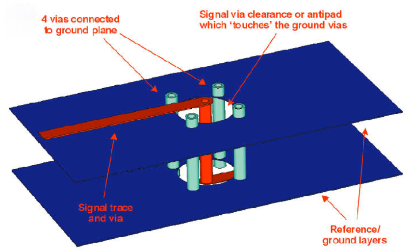
Use Ground Vias for Return Paths
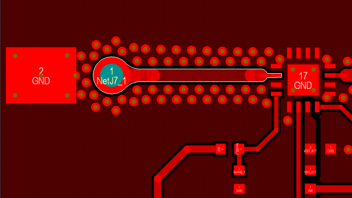
Placing ground vias near signal vias creates a low-inductance return path. This technique, often called RF PCB via stitching, reduces the loop area and minimizes electromagnetic radiation. Ground vias should be positioned symmetrically around signal vias to maintain consistent impedance and suppress noise.
Maintain Impedance Continuity
Vias can disrupt the characteristic impedance of transmission lines. To counteract this, designers must match the via impedance to the trace by adjusting pad sizes and antipad clearances. Simulation tools can help predict impedance changes and guide via design for RF circuits.
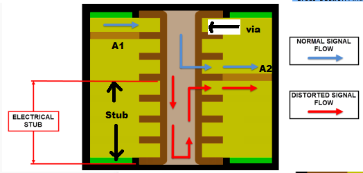
Avoid Via Stubs
Via stubs, or unused portions of a via barrel, act as resonant structures at high frequencies, causing signal reflections. Backdrilling, a process to remove stub sections, is a common solution in RF PCB design. This ensures cleaner signal transmission by eliminating unwanted resonances.
RF PCB Via Placement Strategies
Proper RF PCB via placement is crucial for maintaining signal integrity in high-frequency designs. Vias should be positioned to minimize disruption to signal paths and ground planes. Avoid placing vias directly in the path of critical RF traces, as this can introduce discontinuities. Instead, route signals to vias at points where impedance changes can be managed.
Spacing between signal vias and ground vias must be optimized. Close proximity reduces loop inductance, but overly tight spacing can lead to manufacturing challenges or crosstalk. A balanced grid pattern for via placement often works best, ensuring uniform current distribution and effective shielding. Engineers should also consider thermal and mechanical constraints during placement to prevent stress on the board.
RF PCB Via Stitching for Enhanced Grounding
RF PCB via stitching involves placing multiple ground vias around signal vias or along ground plane edges. This technique creates a robust return path for high-frequency currents, reducing inductance and electromagnetic interference. Stitching vias also help maintain a continuous ground reference, critical for impedance control in RF designs.
The spacing of stitching vias depends on the operating frequency. For higher frequencies, closer spacing is necessary to prevent radiation through gaps in the ground plane. A common guideline is to space vias at intervals less than one-tenth of the wavelength of the highest frequency. This ensures effective shielding and minimizes noise coupling between adjacent signals.
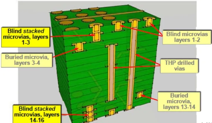
Leveraging RF PCB Blind and Buried Vias
RF PCB blind and buried vias offer advanced solutions for high-density and high-frequency designs. Blind vias connect an outer layer to an inner layer without passing through the entire board, reducing via length and inductance. Buried vias connect internal layers only, further minimizing signal path disruptions and improving layout flexibility.
These via types are particularly useful in multilayer RF PCBs where space is limited. By eliminating unnecessary through-hole vias, blind and buried vias reduce parasitic effects and enable tighter routing. However, they require precise manufacturing processes and adherence to strict design rules to ensure reliability. Engineers must consider aspect ratios and drilling tolerances when implementing these structures.
Related Reading: Unlocking PCB Density: A Beginner's Guide to Blind Vias
Practical Solutions for Signal Integrity in RF PCB Via Design
Achieving maximum signal integrity in RF PCB via design involves combining multiple strategies. Below are actionable solutions for engineers working on high-frequency projects.
Optimize Layer Stack-Up
A well-planned layer stack-up reduces the number of layer transitions, minimizing via usage. Place critical RF signals on outer layers whenever possible to avoid vias altogether. If transitions are unavoidable, ensure ground planes are adjacent to signal layers for effective return paths.
Use Simulation Tools
Electromagnetic simulation helps predict via behavior at high frequencies. By modeling inductance, capacitance, and impedance, engineers can refine via designs before fabrication. This step is essential for complex RF circuits where small errors can have significant impacts.
Follow Industry Standards
Adhering to recognized standards ensures via designs meet performance and reliability criteria. For instance, IPC-2221B provides guidelines on via sizing and spacing for high-speed designs. Compliance with such standards reduces design iterations and improves manufacturability.
Conclusion
RF PCB via design is a critical aspect of high-frequency circuit performance. By focusing on minimizing RF PCB via inductance and optimizing signal integrity, engineers can achieve reliable and efficient designs. Strategies like proper RF PCB via placement, effective via stitching, and the use of blind and buried vias play a vital role in reducing parasitic effects. Adherence to RF PCB via design rules, grounded in industry standards, ensures consistent results in demanding applications. With careful planning and simulation, designers can address challenges and deliver high-quality RF solutions.
FAQs
Q1: How does RF PCB via inductance affect high-frequency signals?
A1: RF PCB via inductance introduces signal delays and reflections, disrupting high-frequency performance. It arises from the via's length and loop area with the return path. Minimizing inductance through shorter vias and ground stitching is essential. This preserves signal integrity, especially in applications like wireless systems where timing and clarity are critical.
Q2: What are the benefits of RF PCB blind and buried vias in design?
A2: RF PCB blind and buried vias reduce via length, lowering inductance and improving signal integrity. They enable denser layouts by connecting specific layers without full board penetration. This minimizes disruptions in multilayer designs. Their use is ideal for compact RF circuits, though manufacturing precision is necessary for reliability.
Q3: Why is RF PCB via stitching important for signal integrity?
A3: RF PCB via stitching creates low-inductance return paths using ground vias near signal vias. It reduces loop area, minimizing electromagnetic interference and noise. This technique maintains impedance continuity at high frequencies. Proper stitching spacing based on wavelength ensures effective shielding in RF designs.
Q4: What are key RF PCB via design rules for minimizing noise?
A4: Key RF PCB via design rules include using short vias to lower inductance and placing ground vias for return paths. Avoid via stubs with backdrilling to prevent resonances. Maintain impedance matching through pad sizing. Following standards like IPC-2221B ensures reliable, noise-free performance in high-frequency circuits.
References
IPC-2221B — Generic Standard on Printed Board Design. IPC, 2012.
IPC-6012E — Qualification and Performance Specification for Rigid Printed Boards. IPC, 2020.
IPC-A-600K — Acceptability of Printed Boards. IPC, 2020.