Introduction
In modern high-speed electronics, PCB stackup design plays a critical role in maintaining signal integrity. Poor stackup choices can lead to signal integrity issues such as crosstalk, impedance mismatch, and reflections, which degrade performance in applications ranging from telecommunications to computing systems. Electrical engineers often encounter these problems during PCB stackup troubleshooting, especially when designs push beyond 1 GHz frequencies. Understanding the interplay between layer arrangement, dielectric materials, and trace geometries is essential for reliable operation. This article explores the causes of these issues, provides structured debugging approaches, and outlines practical resolutions to optimize PCB performance. By addressing signal integrity issues early, engineers can avoid costly respins and ensure compliance with industry expectations.
Understanding PCB Stackup and Signal Integrity
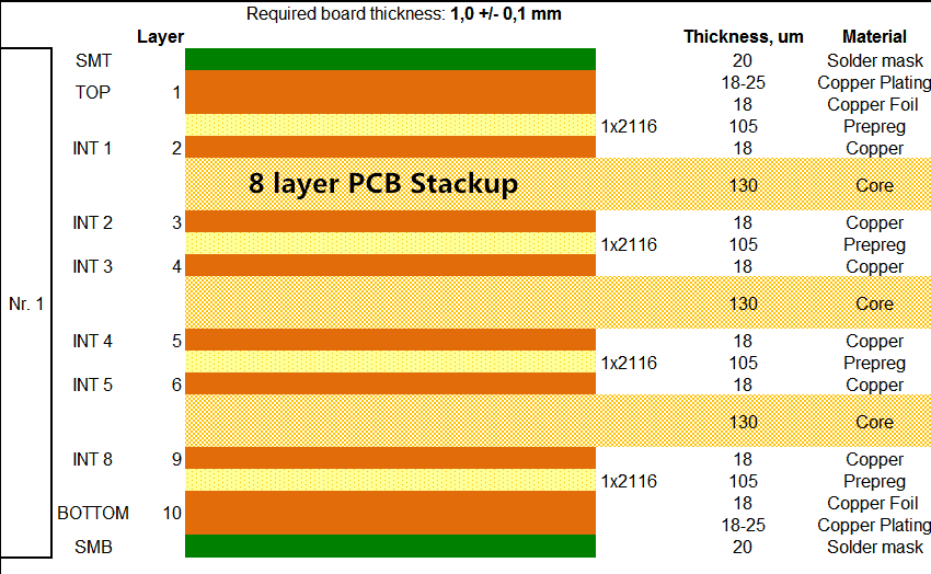
PCB stackup refers to the specific arrangement of conductive layers, dielectrics, and planes within a multilayer board. Each layer contributes to the overall electrical characteristics, including characteristic impedance, propagation delay, and coupling between signals. Signal integrity encompasses the preservation of electrical signal quality from source to receiver, free from distortion or noise. In high-speed designs, stackup directly influences these parameters because dielectric thickness and material properties determine capacitance and inductance per unit length. Improper stackup can amplify signal integrity issues, making it a focal point in PCB stackup troubleshooting.
The relevance of stackup to signal integrity stems from its impact on transmission line behavior. For instance, signals propagating on traces behave as transmission lines when rise times are short relative to trace lengths. Industry guidelines, such as those in IPC-2221, emphasize balanced layer sequencing to support controlled impedance and minimize losses. Engineers must consider factors like core thickness, prepreg stack, and plane proximity during initial design. Neglecting these can result in unexpected crosstalk or reflections during prototyping. Thus, a well-planned stackup serves as the foundation for robust signal performance across frequencies.
Common Causes of Signal Integrity Issues in PCB Stackup
Signal integrity issues often trace back to fundamental stackup flaws that disrupt uniform transmission characteristics. Impedance mismatch occurs when the trace impedance deviates from the driver’s or receiver’s requirements, typically due to inconsistent dielectric heights or material variations across layers. This mismatch creates voltage standing waves, leading to reflections that attenuate the signal and introduce jitter. In multilayer boards, asymmetric stackups exacerbate the problem by causing uneven coupling to reference planes. During PCB stackup troubleshooting, engineers first verify nominal impedance values against design targets.
Reflections primarily arise from discontinuities in the transmission path, such as abrupt changes in trace width, vias, or plane splits influenced by stackup geometry. A via stub extending beyond the signal layer into unused dielectric acts like an open stub resonator, reflecting energy back at specific frequencies. Stackup decisions, like placing signal layers far from ground planes, increase loop inductance and worsen these effects. Reflections manifest as overshoot, undershoot, or ringing on eye diagrams, compromising bit error rates. Debugging requires isolating whether the stackup or routing is the culprit through systematic measurements.
Crosstalk represents inductive and capacitive coupling between adjacent traces, intensified by thin dielectrics or poor plane shielding in the stackup. Near-end crosstalk affects the aggressor trace near the driver, while far-end crosstalk impacts the victim at the receiver end. Dense layer stacks without dedicated ground planes between signal layers amplify mutual inductance, coupling noise onto quiet lines. Signal integrity issues like these become prominent above 500 MHz, where wavelength approaches trace dimensions. IPC-6012 specifications highlight the need for controlled layer interfaces to mitigate such coupling in qualified boards.
Other mechanisms include ground bounce from shared return paths and dielectric losses from high-frequency materials mismatched to the stackup. Warpage from thermal expansion mismatch in asymmetric stacks can alter clearances post-fabrication, indirectly affecting impedance. Engineers debugging these must correlate stackup drawings with fabricated cross-sections. Comprehensive analysis reveals how initial stackup choices propagate through manufacturing tolerances.
Troubleshooting Techniques for PCB Stackup-Related Signal Integrity Problems
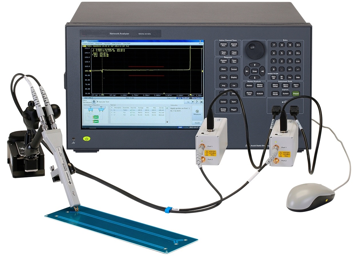
Effective PCB stackup troubleshooting begins with pre-layout simulations to predict impedance profiles and coupling. Field solvers calculate characteristic impedance based on stackup parameters like dielectric constant, thickness, and trace geometry. Discrepancies between simulated and measured values guide stackup revisions. For fabricated boards, time-domain reflectometry (TDR) identifies impedance mismatches and reflections by sending a step signal and analyzing reflections. TDR traces reveal step changes corresponding to layer transitions or vias.
Vector network analysis (VNA) quantifies S-parameters, including insertion loss and return loss, to pinpoint frequency-dependent issues from stackup losses. Crosstalk debugging uses near-end and far-end coupling measurements between aggressor-victim pairs. Eye diagram analysis on oscilloscopes visualizes cumulative distortions from multiple effects. During debugging, engineers isolate stackup contributions by comparing single-ended versus differential signals on varied layer pairs.
Physical inspection complements electrical tests. Cross-sectioning samples measures actual dielectric thicknesses against stackup specs, accounting for resin squeeze-out. Microsection analysis per IPC-A-600 criteria verifies layer registration and plating integrity. Thermal imaging detects hotspots from poor plane distribution in the stackup. Combining these techniques forms a logical progression from simulation to hardware validation.
Systematic debugging workflows prioritize high-risk nets, such as clocks or data buses. Logging measurements against stackup variables enables root-cause mapping. For instance, if reflections correlate with via locations near plane edges, stackup plane extensions provide clues.
Best Practices for Resolving Stackup Signal Integrity Issues
Resolving signal integrity issues demands iterative stackup optimization grounded in engineering principles. Prioritize symmetric stackups to balance expansion and maintain uniform impedance across the board. Place signal layers adjacent to ground or power planes, minimizing distance to 3-5 mils for microstrip or stripline configurations. This setup reduces loop area, suppresses crosstalk, and stabilizes reference for return currents.
Controlled impedance design targets 50 ohms single-ended or 100 ohms differential, calculated from stackup parameters. Adjust trace widths and dielectric thicknesses iteratively, verifying with field solvers. Incorporate stitching vias along plane edges to provide low-inductance returns, mitigating ground bounce. For high-density boards, dedicate inner layers to ground planes, interleaving them with signals to shield against EMI.
Minimize via stubs by back-drilling or using blind/buried vias, preserving stackup integrity. Select low-loss dielectrics with stable Dk/Df for frequencies above 10 GHz, ensuring stackup compatibility. During resolution, prototype varied stackups to benchmark performance metrics like eye height and jitter.
Best practices extend to manufacturing handoff. Specify tolerances tightly, such as ±10% on dielectric thickness, to preserve impedance control. Post-fabrication, verify with flying probe or fixture tests before assembly.
Suggested Reading: PCB Stack Up to Plan, Design, Manufacture and Repeat
Case Study: Debugging Crosstalk in a High-Speed Interface
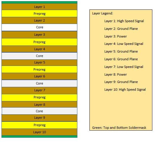
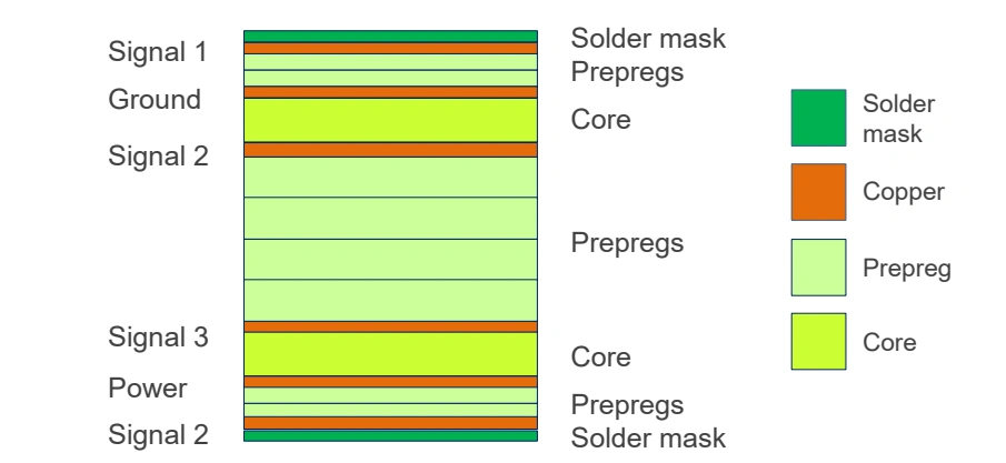
Consider a 16-layer board for a 10 Gbps SerDes interface exhibiting excessive crosstalk during validation. Initial TDR showed nominal 100-ohm differential impedance, but eye diagrams revealed far-end noise closing the eye by 20%. Cross-sectioning revealed 8-mil dielectric between signal layers without intervening ground, violating shielding principles.
Troubleshooting isolated aggressor-victim pairs on adjacent layers. VNA S-parameters confirmed -30 dB coupling at Nyquist frequency. Revising the stackup inserted a ground plane, reducing dielectric spacing to 4 mils per side and crosstalk by 15 dB. Simulations validated the fix pre-spin. This case underscores stackup’s dominance in signal integrity issues resolution.
Conclusion
PCB stackup troubleshooting is indispensable for conquering signal integrity issues like crosstalk, impedance mismatch, and reflections. By mastering stackup fundamentals, employing rigorous debugging tools, and applying proven best practices, electrical engineers can deliver high-performance boards. Symmetric designs with proximate reference planes form the core of reliable solutions. Integrating simulations, measurements, and inspections ensures first-pass success. Ultimately, disciplined stackup management aligns designs with performance goals, reducing debugging cycles and enhancing product reliability.
FAQs
Q1: What are the primary causes of crosstalk in PCB stackup troubleshooting?
A1: Crosstalk arises mainly from capacitive and inductive coupling between traces when signal layers lack sufficient shielding in the stackup. Thin dielectrics or distant ground planes increase mutual coupling, especially for parallel runs longer than one-third wavelength. Debugging involves measuring aggressor-victim S-parameters and verifying plane adjacency. Optimal resolution inserts ground planes between signal layers to confine fields.
Q2: How does impedance mismatch lead to reflections in signal integrity issues?
A2: Impedance mismatch occurs when trace Z0 deviates from source/receiver norms due to stackup variations like uneven prepreg thickness. This causes partial reflections per transmission line theory, manifesting as ringing or jitter. TDR identifies mismatch locations during troubleshooting. Correct by recalculating trace geometries for target impedance using stackup parameters.
Q3: What role do ground planes play in resolving PCB stackup signal integrity problems?
A3: Ground planes adjacent to signal layers provide low-impedance return paths, reducing inductance and crosstalk in stackup designs. They shield against EMI and stabilize impedance. Poor placement amplifies issues; best practice interleaves planes with signals. Verification through VNA return loss confirms effectiveness.
Q4: How can engineers debug reflections effectively in multilayer stackups?
A4: Start with TDR to locate discontinuities like vias or plane splits influenced by stackup. Analyze eye diagrams for cumulative effects and correlate with simulations. Cross-sections validate physical stackup. Mitigate via back-drilling and stitching for clean paths.
References
IPC-2221B — Generic Standard on Printed Board Design. IPC, 2012
IPC-6012E — Qualification and Performance Specification for Rigid Printed Boards. IPC, 2015
IPC-A-600K — Acceptability of Printed Boards. IPC, 2020