Introduction
High-density interconnect (HDI) PCBs enable compact designs with fine-pitch components and microvias, making them essential for modern electronics. In flex and rigid-flex applications, HDI PCB flex and HDI PCB rigid-flex configurations combine these density advantages with mechanical flexibility, supporting devices like wearables, medical implants, and aerospace systems. Flexible circuit design in HDI contexts addresses space constraints while maintaining signal integrity and reliability under bending stresses. Engineers must consider unique challenges such as material selection and via reliability when integrating HDI features into these structures. This article explores structured design principles for HDI PCB flex and rigid-flex boards, drawing on industry standards to guide optimal performance.

Understanding Flexible HDI PCBs in Flex and Rigid-Flex Applications
HDI PCBs incorporate microvias, finer line widths, and higher layer counts compared to standard boards, typically using build-up processes for density. HDI PCB flex refers to fully flexible substrates with HDI features, while HDI PCB rigid-flex hybrids integrate rigid sections for components with flexible transitions for folding. These designs matter in applications requiring 3D packaging, where traditional rigid boards fail due to size or movement. Flexible circuit design allows routing in confined spaces, reducing interconnect lengths and improving electrical performance. Reliability hinges on balancing density with flex endurance, particularly in dynamic environments. Industry adoption grows as components shrink, demanding HDI capabilities in non-planar formats.
Rigid-flex structures often place HDI in rigid areas to leverage microvia stacking, while flex sections prioritize bendability. This segmentation prevents stress concentrations at high-density zones. Engineers benefit from reduced assembly steps, as rigid-flex integrates multiple boards into one unit. Signal integrity improves with shorter paths, minimizing crosstalk in high-speed signals. However, material compatibility and process controls become critical to avoid delamination during flexing.
What Is a Flexible HDI PCB?
A flexible HDI PCB is a flexible printed circuit that incorporates high-density interconnect structures into its layer stackup. Depending on the construction and manufacturing process, these structures can include microvias, blind vias, fine-pitch traces, and compact fanout patterns.
Compared with a conventional flexible circuit PCB, an HDI flex PCB provides additional options for routing signals and connecting components in limited spaces. However, adding HDI features does not eliminate the mechanical requirements of a flex circuit. Via placement, copper distribution, bend radius, and material selection still need to be considered together.
For rigid-flex applications, HDI structures can often be concentrated in rigid sections or other areas with limited mechanical movement. This allows the design to take advantage of high-density routing while keeping the primary flex zones suitable for repeated bending or folding.
HDI Flex PCB vs. Rigid-Flex HDI PCB
An HDI flex PCB uses flexible construction across the circuit, while a rigid-flex HDI PCB combines rigid and flexible sections within the same board structure.
A fully flexible HDI PCB must account for mechanical stress across its flexible layers. Dense via structures and other rigid features therefore require careful placement, particularly when the board is expected to bend repeatedly.
In a rigid-flex HDI design, high-density routing, component placement, and microvia structures can be concentrated in rigid sections, while the flexible sections provide the required mechanical movement. This separation can make it easier to balance high-density interconnect requirements with flex reliability.
The appropriate construction depends on the available space, component arrangement, bending requirements, layer count, signal integrity requirements, and manufacturing process.
Technical Principles of HDI Integration in Flexible PCB Design
HDI integration in flexible PCB design requires more than simply reducing trace width or adding microvias. The complete stackup must support both high-density electrical routing and the mechanical requirements of the flexible structure.
Material selection, copper thickness, dielectric construction, via geometry, and layer arrangement all affect the final performance of a flexible HDI PCB. These factors become particularly important when the board includes high-density routing near a rigid-to-flex transition or a controlled bending region.
Flexible HDI PCB Stackup and Layer Configuration
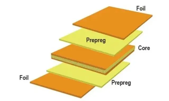
The stackup determines how signals, power, ground, dielectric layers, and HDI structures are distributed throughout the board. In flexible constructions, the stackup must also account for the total thickness and bending behavior of the flex section.
A thinner flex structure generally provides greater flexibility, but reducing thickness can also affect impedance control, mechanical strength, and manufacturing tolerances. Designers should therefore avoid treating flex thickness as an isolated parameter.
For rigid-flex PCB HDI designs, the rigid and flexible portions may use different material constructions while remaining part of the same overall board. The transition between these areas needs to be considered during stackup development to avoid unnecessary mechanical stress.
Microvias and Blind/Buried Vias in Flexible HDI PCBs
Microvias provide a compact connection between adjacent conductive layers and are widely used in HDI structures where routing space is limited. They can reduce the space required for component fanout and help increase routing density in compact designs.
Blind and buried vias can also be used in suitable HDI constructions. A blind via connects an outer layer to one or more internal layers, while a buried via is contained entirely within the internal layer structure.
For flexible circuits, however, via selection must consider mechanical behavior as well as electrical connectivity. Dense via fields or rigid structures located directly within a repeatedly bent area can create local stress concentrations. In rigid-flex HDI designs, blind and buried vias are therefore often better suited to rigid or low-flex regions where mechanical movement is limited.
Via diameter, pad size, copper distribution, dielectric thickness, plating quality, and the distance from the bend area should be evaluated together during design.
HDI Routing Density and Fine-Pitch Fanout
One of the main advantages of HDI technology is the ability to increase routing density without continuously increasing the overall board size. Microvias and fine-pitch fanout structures allow connections to be routed through smaller areas around dense component footprints.
For high-density FPCB designs, this routing strategy must be adapted to the mechanical behavior of the flexible section. Fine traces should follow suitable bend directions, and abrupt geometry changes should be avoided in areas that experience repeated movement.
In rigid-flex boards, dense fanout can generally be concentrated in rigid areas, while the flexible section is used primarily for controlled signal and power routing between rigid regions.

Trace routing in bend regions follows curved paths parallel to the flex axis, distributing strain evenly. HDI PCB rigid-flex stackups layer rigid cores with flex extensions, using coverlays for protection. Via-in-pad designs suit HDI but demand filled vias in flex for planarity. Impedance control challenges arise from varying dielectric thicknesses, requiring simulation for high-frequency signals.
Best Practices for Flexible HDI PCB and Rigid-Flex Design
Successful flexible HDI PCB design requires electrical, mechanical, and manufacturing requirements to be considered at the same time. A layout that achieves high routing density but places excessive stress on the flex section may create reliability problems during assembly or operation.
The following practices help balance HDI density with the mechanical requirements of flexible and rigid-flex boards.
Designing Bend Areas Around HDI Features
Bend areas should be planned early in the layout rather than treated as a final mechanical constraint. Dense microvia fields, large pads, abrupt trace transitions, and other rigid structures should generally be kept away from areas that experience significant or repeated bending.
For compact HDI flex PCB designs, routing density can often be increased by moving high-density structures toward rigid or low-flex regions. This leaves the primary bend zone with a more suitable trace arrangement and reduces the mechanical stress applied to HDI features.
The required clearance from a bend area depends on the stackup, material system, copper thickness, bend radius, and whether the application uses static or dynamic flexing.

Routing and Signal Integrity in High-Density FPCB Designs
High-density FPCB routing requires both electrical and mechanical control. Fine-pitch routing can reduce interconnect length and improve space utilization, but traces in flexible areas still need to accommodate bending without creating excessive strain.
For high-speed or RF applications, designers should also consider controlled impedance, reference-plane continuity, dielectric thickness, trace geometry, and return-current paths. A compact HDI structure should not be introduced in a way that creates an unexpected discontinuity in the signal path.
When blind vias or microvias are used in RF sections, their location and transition geometry should be evaluated together with the surrounding reference structures. This is especially important for precision HDI flex PCB designs where small geometric changes can affect electrical performance.
Managing Rigid-to-Flex Transitions
The rigid-to-flex transition is one of the most important areas in a rigid-flex HDI design. The transition must accommodate differences in material structure and mechanical behavior without creating an abrupt concentration of stress.
Trace routing should be smooth through the transition, and unnecessary copper accumulation should be avoided where it could increase local stiffness. Designers should also consider the relationship between the rigid stackup, flex layers, coverlay, adhesive construction, and bend location.
Keeping dense HDI features within suitable rigid regions can simplify the transition and reduce mechanical stress on vias and fine-pitch structures.
Common Challenges in Flexible HDI PCB Design and Engineering Solutions
Although HDI technology can significantly increase routing density, combining it with flexible construction introduces additional mechanical and manufacturing considerations. Common issues include microvia reliability, copper fatigue, rigid-to-flex transition problems, and insufficient space around bend areas.
Early design-for-manufacturing review can help identify these issues before fabrication and reduce the need for late-stage layout changes.
Via Reliability and Microvia Cracking
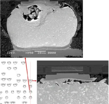
Microvia reliability depends on factors such as aspect ratio, plating quality, pad geometry, dielectric construction, and the manufacturing process. In flexible and rigid-flex boards, mechanical movement adds another factor that needs to be considered.
Microvias positioned too close to repeatedly bending areas may experience additional mechanical stress. Blind and buried vias can also create localized rigid regions depending on their construction and placement.
For this reason, via reliability should be evaluated together with the intended bend behavior rather than only through electrical connectivity. Where possible, high-density via structures should be concentrated in rigid or low-flex regions of a rigid-flex PCB.
Rigid-to-Flex Transition and Delamination
Rigid-to-flex transitions combine materials with different mechanical and thermal characteristics. If the transition is not properly designed or processed, repeated mechanical movement or thermal cycling can contribute to delamination, copper fatigue, or other reliability problems.
A suitable transition design should consider material compatibility, stackup construction, adhesive behavior, copper distribution, and the location of the first major bend.
Manufacturing controls are equally important. Lamination parameters, material handling, drilling, plating, and coverlay processing can all affect the final reliability of the transition.
RF and High-Speed Challenges in Flexible HDI Designs
RF and high-speed circuits introduce additional requirements for flexible HDI PCB design. Changes in dielectric thickness, trace geometry, reference-plane continuity, or via transitions can affect impedance and signal integrity.
For RF applications using blind or microvia structures, the via transition should be considered as part of the complete transmission path. Keeping the signal path compact can be beneficial, but routing density should not compromise the required electrical structure.
A practical design should therefore balance high-density interconnect requirements with controlled impedance, return paths, material characteristics, and the mechanical constraints of the flex section.
Suggested Reading: HDI PCB Design: Overcoming Challenges in High-Density Interconnect
Conclusion
Flexible HDI PCB technology combines high-density interconnect structures with the space-saving and mechanical advantages of flexible circuit construction. Microvias, fine-pitch routing, and optimized stackups can increase routing density, while rigid-flex architectures can separate high-density component areas from regions that require mechanical movement.
The main design challenge is finding the right balance between interconnect density, signal integrity, mechanical flexibility, and manufacturing reliability. Careful control of stackup, via placement, bend areas, rigid-to-flex transitions, and material selection is essential for a reliable HDI flex PCB.
For complex designs, reviewing these requirements during the early design and DFM stages can help ensure that the final flexible or rigid-flex HDI PCB meets both electrical and mechanical requirements.
FAQs
Q1: What materials are best for HDI PCB flex applications?
A1: HDI PCB flex materials like polyimide offer superior thermal resistance and flexibility compared to polyester, supporting microvia processes and repeated bending. Adhesiveless constructions improve reliability by minimizing peel issues. Select based on operating temperature and bend cycles, ensuring compatibility with HDI buildup. IPC-6013 provides qualification criteria for these substrates.
Q2: How does bend radius impact HDI PCB rigid-flex reliability?
A2: HDI PCB bend radius determines fatigue life, with tighter radii increasing copper strain in microvia areas. Design flex zones with adequate radius per application, avoiding HDI features nearby. Static uses allow smaller radii than dynamic ones. Follow IPC-2223 for structured guidelines to prevent cracks.
Q3: What are key design rules for flexible circuit design in HDI PCBs?
A3: Flexible circuit design prioritizes curved traces in bends, microvias in rigid parts, and symmetric stackups for HDI PCB flex. Limit layer count in flex to maintain bendability. Ensure via protection with fills and coverlays. Simulate impedance and strain for optimal performance.
Q4: Can HDI features be fully integrated into pure flex PCBs?
A4: HDI PCB flex supports limited microvias, best in low-flex zones due to strain risks. Rigid-flex hybrids excel for full HDI, combining densities. Material ductility and via sizing control reliability. Reference standards like IPC-2223 for feasible configurations.
Q5: What are the main advantages of using HDI technology in an FPCB?
A5: HDI technology can increase interconnect density without requiring a proportional increase in board size. In an FPCB, this can help accommodate more connections within compact component layouts, reduce the space needed for fanout, and support smaller overall circuit assemblies. The actual benefits depend on the layer structure, component density, manufacturing capabilities, and electrical requirements of the application.
Q6: Does a higher layer count always improve flexible PCB routing?
A6: Not necessarily. Adding layers can provide more routing channels, but it can also increase overall thickness, affect flexibility, and introduce additional manufacturing considerations. The optimal layer count depends on the required routing density, signal integrity, mechanical constraints, component arrangement, and target manufacturing process.
Q7: What factors affect the cost of a high-density FPCB?
A7: The cost of a high-density FPCB depends on several factors, including layer count, material selection, circuit dimensions, copper construction, minimum trace and spacing requirements, via technology, surface finish, and production volume. HDI structures and tighter manufacturing tolerances can increase process complexity, so the cost should be evaluated against the actual routing and space requirements rather than HDI capability alone.
Q8: Is HDI suitable for every flexible PCB application?
A8: No. HDI is most useful when a design has a genuine need for higher interconnect density or space reduction. For relatively simple flexible circuits with sufficient routing space, conventional construction may be more appropriate. The decision should consider electrical requirements, mechanical requirements, available space, manufacturing complexity, and cost.
Q9: What should be included in an HDI flex PCB manufacturing review?
A9: An HDI flex PCB manufacturing review should cover the layer stackup, material construction, minimum trace and spacing, via specifications, copper thickness, bend requirements, rigid-to-flex transitions where applicable, surface finish, and fabrication tolerances. Reviewing these items before production helps identify potential manufacturing constraints and ensures that the design intent can be translated into a manufacturable board.
References
IPC-2223C — Sectional Design Standard for Flexible Printed Boards. IPC, 2019
IPC-6013D — Qualification and Performance Specification for Flexible Printed Boards. IPC, 2014
IPC-6012DS — Qualification and Performance Specification for High Density Interconnect (HDI) Printed Boards. IPC, 2015