










Core Knowledge and Engineering Practices for FPC Design
Flexible printed circuits (FPCs) consist of thin, bendable substrates with conductive traces that enable compact, three-dimensional electronic packaging. Unlike rigid PCBs built on FR4 or similar laminates, FPCs use polymer films such as polyimide (PI) or polyester (PET) that allow repeated flexing or static forming. Key advantages include reduced weight and thickness, the ability to fit into tight or moving assemblies, and support for high-density interconnects without bulky connectors or cables. These characteristics make FPCs essential in space-constrained or motion-intensive applications.
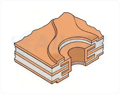
Engineers distinguish between static bend and dynamic flex PCB applications. Static designs involve a one-time or occasional bend during assembly or installation, while dynamic flex requires repeated bending over the product lifetime, often tens of thousands to millions of cycles. The difference drives entirely different material and layout choices.
Industry demand comes from consumer electronics like foldable phones and smartwatches, automotive systems including dashboard displays and sensor harnesses, medical devices such as endoscopes and wearable monitors, aerospace avionics, and industrial automation. In each sector, poor FPC design leads to field failures, warranty claims, and delayed time-to-market.
This guide compiles practical design rules drawn from factory CAM experience, DFM reviews, and reliability testing. It covers material selection, bend region optimization, impedance control, application-specific considerations, and real production cases. Following these guidelines helps reduce defect rates, improve yields, and streamline RFQ processes for both designers and manufacturers.
Material Selection as the Foundation of FPC Design
Material selection is one of the earliest and most critical decisions in flexible circuit design. Unlike rigid PCBs, the mechanical performance, bend reliability, thermal resistance, and manufacturing cost of an FPC are heavily influenced by the material system chosen before layout begins. An inappropriate material choice can lead to premature fatigue failures, delamination, impedance instability, or assembly defects regardless of how well the circuit is routed.
Substrate Material Selection: PI vs PET
|
Property |
Polyimide (PI) |
Polyester (PET) |
|---|---|---|
|
Temperature Resistance |
Excellent (>300°C thermal stability) |
Limited temperature resistance |
|
Flexibility |
Excellent |
Good |
|
Dimensional Stability |
Excellent |
Moderate |
|
Reflow Soldering Compatibility |
Suitable |
Generally unsuitable |
|
Reliability |
High |
Moderate |
|
Typical Applications |
Automotive, aerospace, industrial, medical electronics |
Consumer electronics, low-cost products |
|
Cost |
Higher |
Lower |
|
Recommended For |
High-reliability and demanding environments |
Cost-sensitive static applications |
PI remains the dominant substrate material for professional FPC designs because it combines thermal stability, mechanical durability, and long-term reliability. PET is primarily used when cost reduction outweighs performance requirements.
Polyimide is widely used in demanding flexible circuits because it offers good thermal stability, dimensional stability, and flexibility. It is suitable for applications that involve repeated bending, higher operating temperatures, or more demanding assembly processes.
Polyester, commonly known as PET, may be suitable for simpler and more cost-sensitive flexible circuits. It is often used in applications where the circuit has limited movement and does not need to withstand high-temperature processing.
The substrate should be selected according to the actual application rather than price alone. Designers should review operating temperature, bend requirements, dielectric performance, and assembly conditions before choosing the material.
Copper Foil Selection: RA vs ED Copper
|
Property |
Rolled Annealed (RA) Copper |
Electrodeposited (ED) Copper |
|---|---|---|
|
Grain Structure |
Horizontal elongated grains |
Vertical columnar grains |
|
Ductility |
Excellent |
Moderate |
|
Dynamic Flex Performance |
Excellent |
Limited |
|
Fatigue Resistance |
High |
Lower |
|
Repeated Bend Cycles |
Suitable |
Not recommended |
|
Static Flex Applications |
Suitable |
Suitable |
|
Cost |
Higher |
Lower |
|
Recommended For |
Dynamic flex circuits and high-cycle bending |
Static flex and cost-sensitive designs |
Copper type is another important consideration in FPC design.
Dynamic flex circuits should generally use RA copper because its grain structure better withstands cyclic mechanical stress. While ED copper is widely used in static flex applications, repeated bending can accelerate fatigue cracking and reduce service life.
Designers must also evaluate whether to use adhesive-based or adhesiveless constructions. Adhesiveless laminates bond copper directly to the polyimide film, reducing overall thickness while improving thermal performance and bend life. These constructions are commonly recommended for high-density designs and dynamic flex regions. Adhesive-based materials remain widely used in cost-sensitive applications but typically exhibit lower long-term flex reliability.
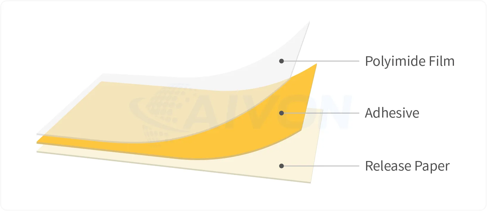
Coverlay, Adhesive, and Stiffener Selection
Coverlay protects the copper traces and provides electrical insulation. Its thickness and opening design affect flexibility, bend performance, pad access, and assembly.
Adhesive-based and adhesiveless constructions may have different mechanical and dimensional characteristics. Designers should confirm which construction is suitable for the intended application.
Stiffeners are often added beneath connectors, component areas, or contact pads. They improve local support and help prevent damage during assembly or insertion. However, stiffeners also increase local thickness and may affect the bend transition.
In flexible PCB design, stiffeners should be placed only where mechanical reinforcement is needed. The transition between stiffened and flexible areas should be designed smoothly to avoid concentrated stress.
FPC Design Fundamental Rules
The main FPC design rules focus on controlling mechanical stress, protecting conductors, and maintaining manufacturable geometry. A flex circuit should not be treated as a rigid PCB that is simply made thinner.
Basic Layout Rules
Basic layout rules form the foundation of manufacturable and reliable FPC designs. Minimum trace width and spacing are typically 75 µm-100 µm for standard production volumes, with advanced processes supporting 50 µm or finer in prototype quantities. These limits depend heavily on copper thickness and chosen fabricator capabilities, so always confirm with your manufacturer rather than assuming generic values. In high-current areas, widen traces or use copper pours while maintaining flexibility; in signal layers, control impedance by adjusting width and reference plane distance.
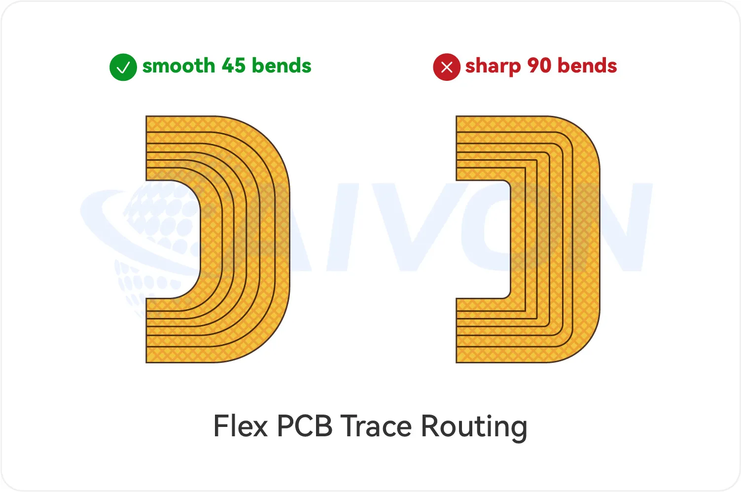
Trace routing in flex areas should prioritize straight runs perpendicular to the bend axis to minimize strain. When perpendicular routing is impossible, use gentle arcs with radius at least 2× trace width. Stagger traces in differential pairs or multi-layer bundles to prevent overlapping stress points during repeated bending. Implement teardrops on all pads (minimum 50% extension) to strengthen the trace-pad junction and compensate for registration tolerances. All trace corners must use a minimum 45° chamfer or full radius — sharp 90° corners act as stress concentrators and frequently initiate copper cracks under dynamic flex.
Component pads in flex zones should be reinforced with local stiffeners, and keep large components or connectors away from bend areas. Proper Flexible PCB connector design is also important when the circuit uses an FPC ZIF connector, as interface selection, contact geometry, ZIF vs LIF requirements, and Gold finger design can all affect assembly reliability. Fiducials for assembly and inspection must be placed in rigid or semi-rigid zones with sufficient clearance. Panelization features such as mouse bites, stamp holes, or V-scores require careful positioning to avoid interfering with functional flexing areas. Following these rules consistently prevents common issues like trace fracturing, pad lifting, and registration-related defects during lamination and coverlay application.
Stack-up design principles
The stack-up determines the overall thickness, flexibility, electrical performance, and mechanical behavior of a flexible circuit. A suitable flexible PCB stack-up design should balance copper distribution, dielectric thickness, coverlay, adhesive, and reinforcement.
Single-layer flexible circuits are often used for simple routing, lightweight interconnects, and applications with limited electrical complexity. They generally provide good flexibility and can be easier to manufacture.

Double-layer flexible circuits provide more routing space and may support better grounding or signal distribution. However, the additional copper and dielectric layers increase total thickness and may reduce bend flexibility.
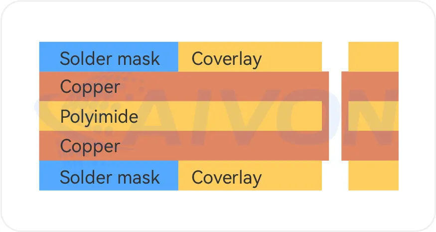
Multilayer flexible PCB design is useful when the circuit requires higher routing density, controlled impedance, shielding, or more complex interconnections.
However, additional layers increase the total thickness and can make the circuit less flexible. The stack-up should therefore be designed around the actual mechanical requirements.
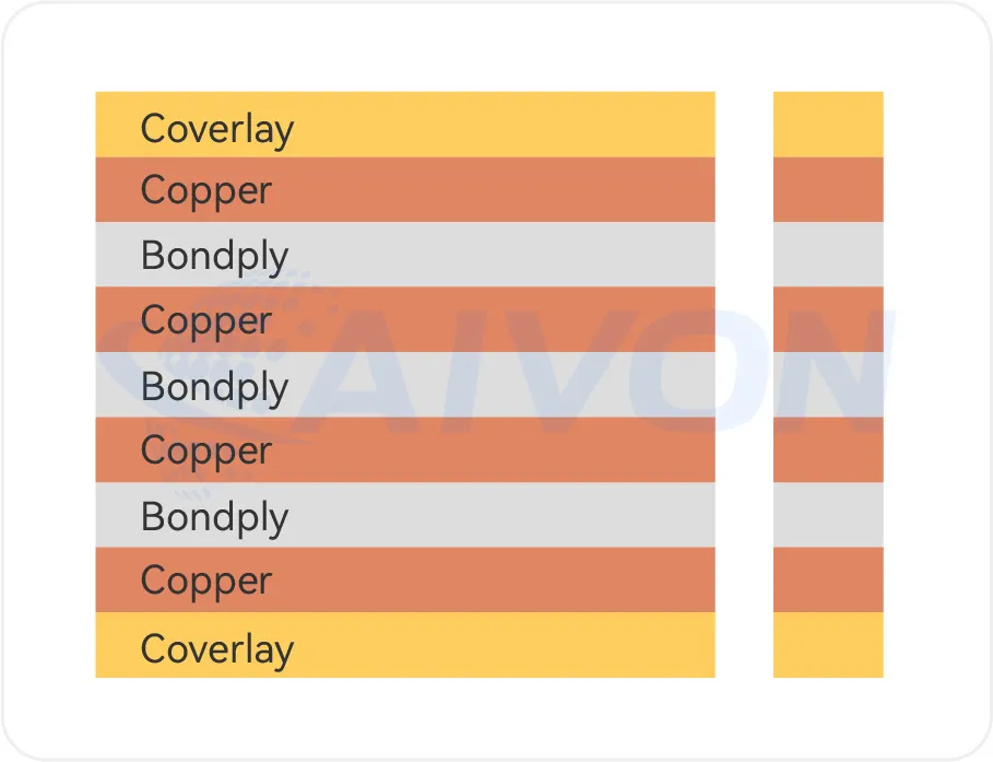
Key principles include placing critical high-speed signals on inner layers when possible for better protection, using adhesiveless materials for thinner profiles and superior flex life, and carefully managing dielectric thicknesses for impedance targets. In rigid-flex designs, transition zones should gradually change layer count and stiffness with stepped or tapered copper removal to avoid abrupt stress changes that cause delamination.
Flexible PCB copper thickness selection follows a clear tradeoff: 12 µm or 18 µm for high-flex applications, 35 µm or heavier for power distribution. FPC copper thinning can help reduce bending strain in demanding flex areas, but the final design must still balance Flexible PCB trace width, current-carrying requirements, and copper thickness impedance. Total stack thickness in dynamic bend areas should stay below 0.15–0.25 mm for optimal performance. Always simulate the complete stack-up for both electrical (impedance, crosstalk) and mechanical (bend stress) performance. Unbalanced or overly thick stack-ups commonly cause warpage, coverlay wrinkling, or reduced flex endurance that only becomes evident after environmental testing.
Grounding and Shielding Strategies
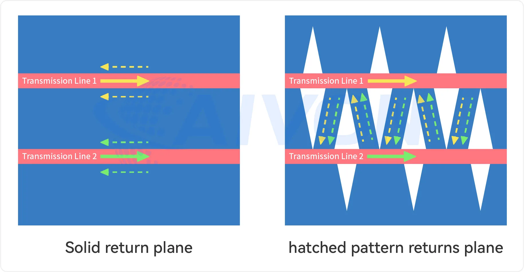
Effective grounding and shielding are essential for maintaining signal integrity and EMI/EMC performance in FPC designs, particularly in high-speed or noise-sensitive applications. In flexible circuits, ground planes should be implemented as continuous copper pours on one or both sides of signal layers whenever possible, with strategic cross-hatching only when full planes would excessively reduce flexibility.

Solid ground planes provide the best return paths and shielding but increase stiffness; hatched patterns (typically 45-60% copper coverage) offer a compromise for dynamic flex zones while still controlling impedance and reducing crosstalk.
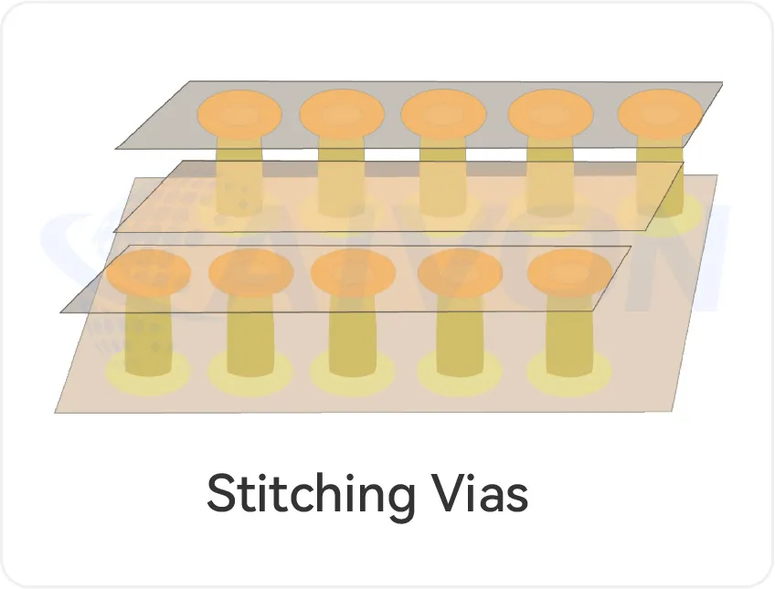
Stitching vias or conductive adhesive between ground layers in multilayer FPCs ensure low-impedance connections across the stack-up. In bend areas, avoid breaking ground continuity—route ground traces or planes to follow the neutral bend axis where mechanical strain is minimal.
For EMI shielding, consider additional silver ink shielding layers, copper foil tapes, or dedicated shield films bonded to the coverlay, especially in wearable and medical devices where external interference or patient safety is critical. Always verify shielding effectiveness through radiated emission testing and maintain ground return paths as short and wide as possible to minimize loop inductance. Poor grounding frequently leads to signal noise, radiated emissions failures, or ground bounce issues that only appear during system-level integration.
Via and Pad Design Guidelines
Via and pad design in FPCs requires special attention due to the mechanical stresses unique to flexible materials. Use teardrop pads at all trace-to-pad junctions to prevent trace necking and pad lifting during bending or thermal expansion.

Minimum annular ring is typically 0.075-0.1mm for reliable plating, with larger rings (0.15 mm+) recommended in high-reliability or dynamic applications.

Plated through holes (PTH) should maintain a hole-to-pad ratio that accounts for drill wander and registration tolerances common in flex processing. Blind and buried vias improve density in multilayer designs but increase cost and require careful aspect ratio control. 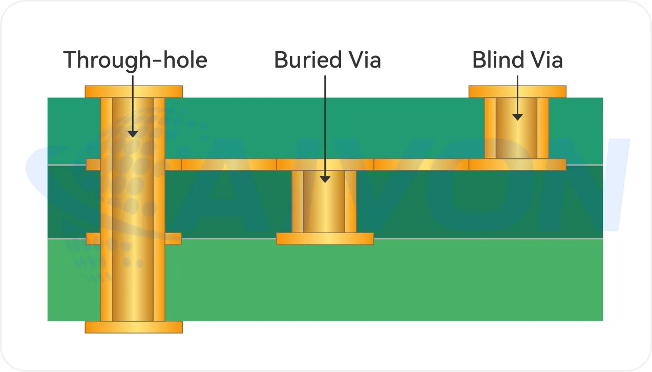
Never place vias directly in dynamic bend zones, as the plating barrel experiences high strain and cracks easily. If vias are unavoidable near bend areas, position them in reinforced static regions and add extra coverlay or stiffener support. Pad shapes should favor rounded or oblong geometries in flex zones to distribute stress. During DFM review, check for via tenting consistency and solder mask or coverlay clearance to avoid solder wicking or shorting risks.
Ignoring these guidelines commonly results in annular ring breakout, via barrel fractures under flexing, or assembly defects that reduce yield and long-term reliability. In production, cross-section analysis of vias is a standard validation step to confirm plating quality before committing to volume.
Bend Area Design Principles
The bend area is the highest-risk zone in most FPC designs. Proper FPC bend radius selection and Flexible PCB stress relief directly determine whether the circuit will survive its intended lifetime or fail prematurely in the field.
Static vs Dynamic Bend Requirements
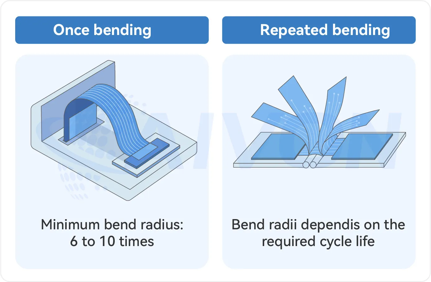
For static bend applications, where the FPC is bent once during assembly or installation and remains in a fixed shape, the minimum bend radius is typically 6 to 10 times the total circuit thickness. This is relatively forgiving and allows more compact designs.
For dynamic flex applications, such as foldable wearables, hinge mechanisms, or sliding assemblies that experience repeated bending, the requirements are much stricter. Recommended bend radii are often 100 times the total thickness or greater, depending on the required cycle life. A design targeting hundreds of thousands of cycles may need a noticeably larger radius than one intended for only a few thousand movements.
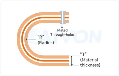
In practice, we evaluate the bend radius together with the overall stack thickness, copper type, and application environment during DFM reviews. Overly aggressive (too small) bend radii are one of the most common causes of early field failures.
Designing Smooth Bend Transitions
In FPC design, smooth transitions are critical in areas where the circuit changes from a flat section to a bend zone, or where local stiffness varies due to coverlay, copper thickness, or stiffener placement. Poorly designed transitions often become stress concentration points and lead to copper cracking or delamination over time.
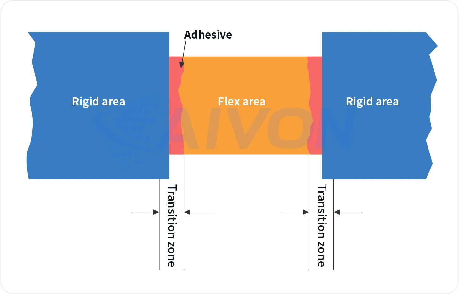
Key Considerations for Smooth Bend Transitions:
● Gradual Change in Stiffness: Avoid abrupt changes in the stack-up or coverlay at the start and end of bend areas. Use tapered coverlay edges or gradually adjust copper density to create a smoother mechanical transition.
● Transition Zone Length: Provide enough length between the flat area and the actual bend radius. A short or sharp transition increases localized stress. In most cases, a transition zone of several millimeters helps distribute strain more evenly.
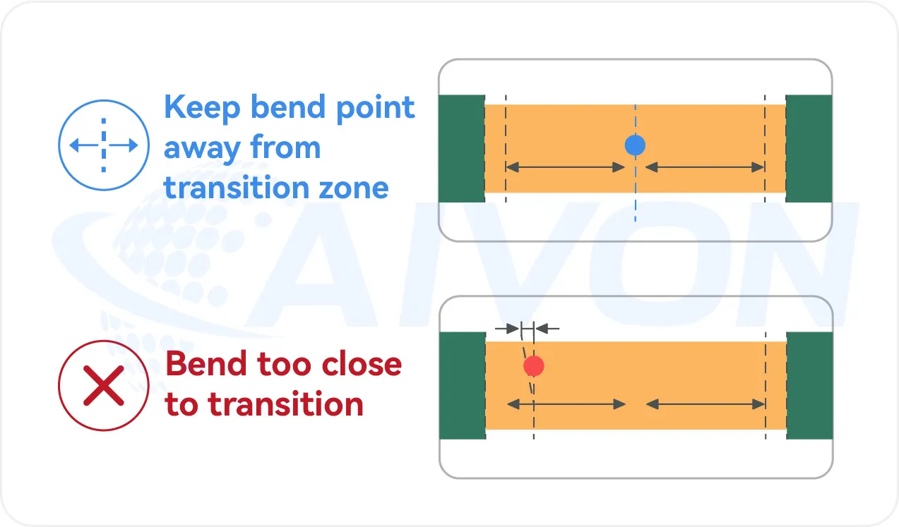
● Trace and Feature Management: Keep critical traces, vias, and pads away from transition boundaries. Route traces perpendicular to the transition line when possible, and avoid sudden width changes near the bend entry point.Strain Relief Features: Add tear stops, rounded corners, or slight relief slots at transition edges to prevent tears from initiating and propagating into functional areas.
● Coverlay and Copper Optimization: In high-cycle applications, consider slightly thicker coverlay or localized reinforcement in transition zones to improve durability without overly restricting flexibility.
When laying out FPCs, always define clear bend zones and transition zones in the mechanical layers. During DFM review, check whether the transition from flat to bend is too abrupt. For demanding dynamic applications, it is recommended to validate the transition design through prototype bending tests, as simulation alone often underestimates the stress at these boundary areas.
Well-executed bend transitions significantly improve the long-term reliability of flexible circuits, especially in products that require repeated flexing.
Impedance Control in Flexible PCB Design
Impedance control in flexible circuits is more challenging than on rigid boards because the materials and geometry can change during bending and manufacturing. Several key factors directly influence impedance in FPC designs:
Main Factors Affecting Impedance Control:
|
Factor |
Description |
Impact on Impedance |
Design Consideration |
|---|---|---|---|
|
Dielectric Thickness |
Thickness of substrate and coverlay |
Directly affects characteristic impedance |
Control coverlay thickness tolerance tightly |
|
Coverlay & Adhesive |
Coverlay material, thickness, and adhesive flow during lamination |
Can shift impedance by 5–10% |
Specify tight coverlay tolerances; validate with TDR |
|
Trace Geometry |
Trace width, spacing, and copper thickness |
Determines target impedance value |
Adjust trace width according to copper thickness and target Zo |
|
Configuration Type |
Microstrip (outer layer) vs Stripline (inner layer) |
Different behavior due to dielectric environment |
Choose configuration based on layer and shielding needs |
|
Bend Area Effects |
Stretching or compression of substrate during bending |
Changes differential pair spacing |
Maintain consistent spacing; avoid critical signals in tight bend zones |
|
Material Variation |
Variations in dielectric constant and copper thickness |
Causes deviation between simulation and actual |
Correlate simulation with prototype TDR measurements |
Practical Recommendations
Because of these variables, simulation tools (such as HyperLynx or SIwave) provide a good starting point but are not sufficient by themselves. In real FPC production, coverlay thickness variation and adhesive flow often cause the actual impedance to deviate from simulation results.
For critical designs, it is recommended to:
● Define clear impedance requirements early in the stack-up stage
● Run simulation and then validate with TDR testing on prototypes
● Work closely with the fabricator to confirm achievable tolerances on coverlay and dielectric thickness
● This approach helps achieve more reliable and repeatable impedance control in flexible printed circuits.
FPC Design Guidelines for DFM and Manufacturing
A practical CAD workflow for FPC starts with importing accurate mechanical constraints and clearly marking all bend zones, fold lines, and stiffener locations as mechanical layers. Define flex-specific design rules early for trace width, spacing, annular rings, and keep-out areas. After routing and stack-up finalization, the most critical phase begins: a thorough DFM review. This final checkpoint determines whether the design will move smoothly into production or require costly iterations.
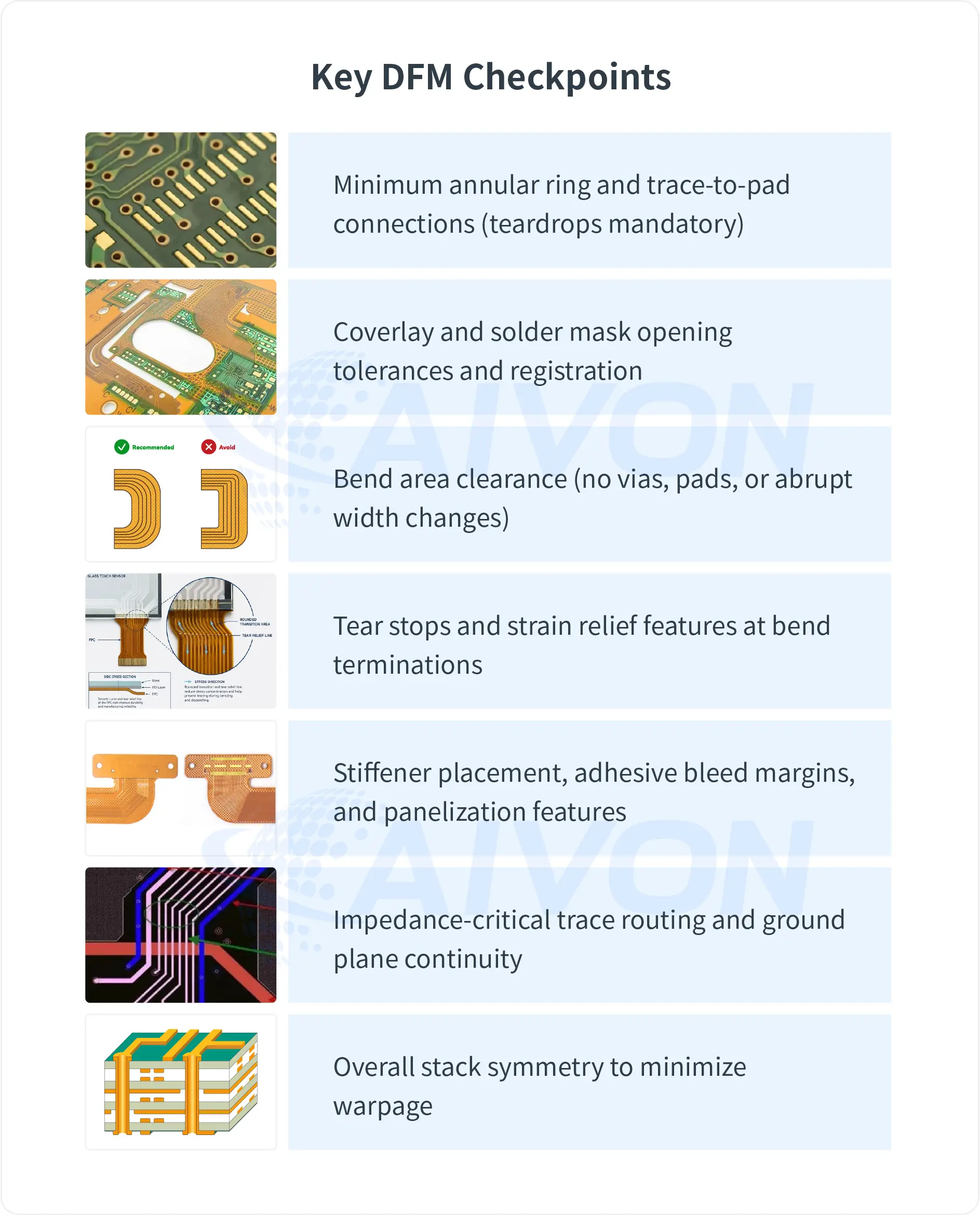
Flex PCB DFM Checklist:
|
Item |
Requirement |
Typical Tolerance/Note |
|---|---|---|
|
Trace Width / Spacing |
75 µm — 100 µm |
Confirm with fabricator capability |
|
Annular Ring |
≥0.1 mm |
0.15 mm preferred for dynamic areas |
|
Teardrops |
Required on all pads |
Minimum 50% extension |
|
Bend Radius |
Static: 6–10× thickness Dynamic: ≥100× thickness |
Validate with target cycle count |
|
Via Placement |
No vias in dynamic bend zones |
Allowed only in reinforced static areas |
|
Coverlay Registration |
±0.075–0.1 mm |
Critical for exposed traces |
|
Panelization |
Fiducials, tooling holes, mouse bites |
Avoid interfering with flex areas |
|
Impedance Control |
±10% target |
Document required layers and structures |
|
Stiffener Alignment |
±0.1 mm |
Adhesive flow control |
This structured final checkpoint, aligned with IPC standards, has proven to be the most effective way to catch issues that would otherwise surface only after fabrication or during reliability testing. Following this process consistently helps achieve higher first-pass yield and shorter overall development time.
IPC Standards for Flexible Circuit Design
|
Standard |
Purpose |
Key Relevance to FPC Design |
|---|---|---|
|
IPC-2223 |
Design Standard for Flexible Printed Boards |
Bend area rules, stack-up guidelines, material selection |
|
IPC-6013 |
Qualification and Performance Specification for Flexible Printed Boards |
Acceptance criteria, reliability test methods |
|
IPC-TM-650 |
Test Methods Manual |
Dynamic bend testing, thermal stress, solderability |
|
IPC-2221 |
Generic Standard on Printed Board Design |
General requirements (used in conjunction with 2223) |
|
IPC-6012 |
Qualification for Rigid Boards |
Applicable to rigid portions of rigid-flex designs |
Flexible PCB Design for Different Applications

Wearable Flexible PCB Design
Wearable devices demand ultra-thin profiles, skin conformability, and sweat resistance. Flexible PCB for wearable electronics must also support high-density layouts with fine-pitch traces and multiple sensors. Material selection often favors thin RA copper on PI with specialized coverlays or soldermask alternatives to maintain flexibility. Dynamic bending occurs around the wrist or joint areas, requiring careful bend-radius control and trace routing.
Automotive Flexible Circuit Design
The Automotive multilayer flexible PCB faces wide temperature ranges, vibration, and AEC-Q100/200 qualification. Designs incorporate thicker copper for current carrying in power distribution or high-reliability materials for sensors and cameras. Vibration-resistant stiffeners and redundant traces improve robustness. Manufacturing must include enhanced thermal cycling and vibration testing.
Medical Flexible PCB Design
Medical FPCs prioritize biocompatibility, miniaturization, and sterilization compatibility. Single-use devices favor cost-optimized constructions, while reusable ones need robust dynamic performance. ISO 10993 and other standards apply. Miniaturization pushes via and trace limits, making DFM collaboration with the manufacturer essential early in development.
Manufacturing practices
Roll-to-roll (R2R) processing enables high-volume, cost-effective production for simpler designs. Laser drilling, precise coverlay alignment, and automated stiffener attachment are critical. Impedance testing, AOI, X-ray, and sample bend testing form part of quality controls. Electrical testing under flex conditions is increasingly common for dynamic applications.
Process choices affect yield-cost balance. Early DFM collaboration with the fabricator prevents costly iterations.
AIVON Flexible PCB Design and Manufacturing Case Studies
Case 1. Large FPC Panel Design Caused Manufacturing and SMT Risks
A customer designed a long 1 × 30 flexible PCB panel to simplify SMT assembly. While the layout appeared efficient from an assembly perspective, it exceeded the optimal manufacturing panel size for FPC production. The oversized panel left insufficient space for tooling holes, reduced material utilization, and introduced significant dimensional variation during lamination and routing.
Without adequate process rails and breakaway connections, the finished panels also became unstable after routing, making SMT handling difficult and increasing the risk of deformation.
AIVON Engineering Solution
Rather than rejecting the design, AIVON's engineering team reviewed the entire manufacturing workflow and proposed a production-friendly panel redesign.
The optimized solution included:
● Reducing the panel size to improve dimensional stability
● Adding process rails at both ends of the panel
● Introducing multiple breakaway tabs along the outline
● Reserving sufficient space for tooling holes and SMT fixtures
● Reinforcing panel edges with copper balancing where necessary
This redesign maintained assembly efficiency while significantly improving manufacturing yield, handling stability, and SMT reliability.
Design takeaway:
FPC panelization should consider both SMT efficiency and manufacturing capability. Proper process rails, breakaway tabs, and tooling clearance are essential for stable production.
Case 2. Copper and Coverlay Design Increased the Risk of Shorts and Assembly Defects
Another customer submitted an FPC design with several manufacturability issues:
● Copper traces extended almost flush with the routed board edge.
● Coverlay openings were significantly larger than the stencil apertures.
● Silkscreen text was placed extremely close to solderable pads.
During manufacturing, these conditions could lead to exposed copper after routing, solder bridging, coverlay misalignment, and silkscreen contamination of solder joints.
AIVON Engineering Solution
After reviewing the Gerber files, AIVON engineers optimized the fabrication data by:
● Increasing copper-to-outline clearance
● Adjusting coverlay openings to appropriate manufacturing tolerances
● Aligning coverlay windows with assembly requirements
● Relocating silkscreen away from solderable areas
● Applying standard manufacturing compensation for coverlay registration
The revised design eliminated potential short circuits and significantly improved soldering consistency without affecting the customer's electrical design.
Design takeaway:
Copper clearance, coverlay opening dimensions, and silkscreen placement should be evaluated together rather than independently. Small layout decisions can have a major impact on assembly yield.
Case 3. Stackup Selection Could Not Meet Both Thickness and Copper Requirements
A customer specified the following stackup:
● 1 oz copper
● White coverlay on both sides
● Finished thickness of 0.20 mm
Although each requirement appeared reasonable individually, the combination exceeded the physical thickness budget. The dual white coverlay layers added additional coating thickness that prevented the requested finished thickness from being achieved within manufacturing tolerance.
Similar cases also involved requests for 1.5 oz copper combined with ultra-thin flexible constructions.
AIVON Engineering Solution
Instead of simply reporting the design as unmanufacturable, AIVON engineers analyzed the stackup and proposed several alternatives.
Depending on the application, recommendations included:
● Adjusting the finished thickness tolerance to a manufacturable range
● Optimizing copper weight according to current-carrying requirements
● Selecting alternative coverlay constructions where appropriate
● Rebuilding the stackup to balance flexibility, thickness, and reliability
By validating the complete stackup before production, the customer avoided costly redesigns and ensured that both electrical and mechanical requirements could be achieved.
Design takeaway:
Flexible PCB stackup parameters, including copper weight, coverlay, adhesive layers, and finished thickness, must be evaluated as an integrated system rather than specified independently.
Common FPC Design Mistakes and How to Avoid Them
|
Mistake |
Root Cause |
Risk |
Consequence |
Recommended Fix |
|---|---|---|---|---|
|
Placing vias or pads in bend zones |
Overlooking mechanical stress in layout |
High stress concentration |
Via cracking, trace fracture, open circuits |
Keep bend areas free of vias/pads; route traces perpendicular to bend |
|
Using ED copper in high-cycle dynamic applications |
Cost-driven material selection without flex life analysis |
Rapid fatigue |
Early field failures |
Specify RA copper for dynamic zones; validate with IPC-TM-650 testing |
|
Insufficient bend radius |
CAD looks fine but ignores total stack thickness |
Copper strain exceeds limits |
Cracking after limited cycles |
Apply 6-10× for static, ≥100× guideline for dynamic; calculate per construction |
|
Sharp trace corners or no teardrops |
Ignoring stress risers |
Localized cracking |
Intermittent opens or shorts |
Always use rounded corners and teardrops |
|
Poor rigid-flex transition design |
Abrupt mechanical and impedance changes |
Delamination, impedance mismatch |
Signal integrity failures |
Gradual transitions, reinforcement, simulation validation |
|
Ignoring coverlay registration tolerances |
Assuming perfect alignment |
Exposed traces or shorts |
Yield loss, reliability issues |
Add generous tolerances and review with manufacturer |
|
Inadequate stiffener placement |
Component mounting without support |
Solder joint fatigue |
Broken connections |
Place stiffeners under all heavy components |
|
Skipping TDR validation |
Relying solely on simulation |
Undetected discontinuities |
System-level signal problems |
Perform TDR on prototypes and production samples |
Conclusion
Effective FPC design balances electrical performance, mechanical reliability, and manufacturability. The bend region remains the critical failure zone in most applications—get the radius, material, and routing correct and you avoid the majority of problems. Material selection, especially copper type and construction method, determines whether your product survives qualification or reaches the field only to return under warranty.
Real manufacturing data shows that designs developed in close collaboration with experienced fabricators achieve higher yields and faster ramps to volume. Early DFM reviews catch issues that CAD tools alone miss.
For your next project, consider submitting files for a complimentary DFM review. Our engineering team can provide stack-up recommendations, bend optimization, and impedance modeling tailored to your application.
FPC Design Frequently Asked Questions
Q1: How is minimum dynamic bend radius calculated for FPC?
A1: Use total circuit thickness multiplied by a factor derived from required cycle life, copper thickness, and material. Consult manufacturer-specific tables or run IPC-TM-650 testing. A common empirical rule is radius ≥ 100 × total thickness for high-cycle applications, adjusted by material data and testing. Use finite element modeling for complex geometries and always validate with physical samples.
Q2: What are the differences between RA and ED copper in flex applications?
A2: RA copper offers superior ductility and fatigue resistance due to its aligned grain structure. ED copper is cheaper and sufficient for static or low-cycle use but shows earlier crack initiation under repeated strain. Choose RA for any dynamic requirement exceeding a few thousand cycles.
Q3: How to achieve 50Ω/100Ω impedance control in FPC?
A3: Control dielectric thickness, trace width/spacing, and reference plane proximity tightly. Use simulation tools, specify tight tolerances on coverlay, and verify with TDR. Adhesiveless constructions provide more predictable results.
Q4: What failures result from common mistakes like sharp trace corners or missing teardrops?
A4: Stress risers initiate cracks that propagate through copper, causing opens. Missing teardrops lead to pad lifting or trace breakout, especially during flex or thermal stress.
Q5: How to choose between FPC and Rigid-Flex?
A5: Choose pure FPC for cost efficiency and simple designs when dynamic flex or tight packaging is needed without dense components on the flexible portion. Choose Rigid-Flex when components must reside on the flexible part or when multiple rigid sections are required.
Q6: What special certifications are required for medical/automotive FPC?
A6: Automotive FPCs require IATF 16949 quality management systems, ISO 26262 functional safety standards, AEC-Q100/200 series standards, and application-specific reliability testing. Medical FPCs typically require ISO 13485 manufacturing controls and biocompatibility compliance per ISO 10993. Both applications require detailed process validation and traceability.
Q7: What are the basic rules for flexible PCB design?
A7: The basic rules for flexible PCB design include selecting suitable materials, defining bend zones, using smooth trace routing, avoiding sharp corners, keeping vias and large components away from dynamic bend areas, and confirming trace width, spacing, coverlay clearance, and stack-up requirements with the manufacturer.
Q8: What is the difference between FPC design and rigid PCB design?
A8: FPC design must consider both electrical and mechanical behavior. Unlike rigid PCB design, flexible circuits may bend, twist, or move during operation. Designers therefore need to evaluate bend radius, copper type, substrate thickness, coverlay, stiffeners, and transition zones in addition to standard layout requirements.
Q9: How do you design a flex PCB?
A9: To design a flex PCB, first define the mechanical envelope, bend zones, and electrical requirements. Then select the substrate, copper type, coverlay, and stiffeners. During layout, use smooth trace paths, avoid placing vias in dynamic bend areas, provide a suitable bend radius, and review the complete stack-up. A flex PCB design DFM review should be completed before fabrication.
Q10: What are the most important FPC design guidelines?
A10: The most important FPC design guidelines include selecting materials according to static or dynamic bending requirements, keeping traces smooth and avoiding sharp corners, avoiding vias and large components in repeated bend areas, using suitable copper thickness and copper type, maintaining an appropriate bend radius, managing coverlay, stiffener, and rigid-flex transition areas, confirming manufacturing tolerances with the fabricator, and validating demanding designs through prototype and reliability testing.
Q11: What is the recommended bend radius for a flexible PCB?
A11: The recommended bend radius depends on the total circuit thickness, copper type, material construction, bend direction, and expected bending cycles. Static-bend applications generally allow a tighter radius than dynamic-flex applications. For repeated bending, designers should use construction-specific guidance from the manufacturer and validate the design through mechanical testing.
Q12: Can vias be placed in a flexible PCB bend area?
A12: Vias should generally be kept out of demanding dynamic bend areas because the plated structure can experience repeated mechanical strain. If a via must be placed near a bend, it should be located in a relatively stable or reinforced area with suitable clearance and mechanical support.
Q13: How does copper thickness affect flexible PCB design?
A13: Copper thickness affects flexibility, trace width, current-carrying capacity, impedance, and manufacturing capability. Thinner copper may improve bend performance and fine-line routing, while thicker copper can support higher current. The final choice should balance electrical requirements with total stack thickness, bend radius, copper type, and reliability expectations.
Q14: What materials are commonly used in FPC design?
A14: Common materials used in FPC design include polyimide, polyester, rolled-annealed copper, electrodeposited copper, coverlay, adhesives, and stiffeners. Polyimide and RA copper are often selected for demanding flexible applications, while PET and ED copper may be suitable for certain static or cost-sensitive designs.
Q15: What is the role of DFM in flexible PCB design?
A15: DFM helps verify whether a flexible circuit can be manufactured consistently. An FPC DFM review normally checks trace width and spacing, copper-to-edge clearance, coverlay registration, bend-zone layout, via placement, stiffener alignment, panelization, stack-up thickness, and assembly requirements.
Q16: What standards are used for flexible circuit board design?
A16: IPC-2223 is commonly referenced for flexible printed board design, while IPC-6013 covers qualification and performance requirements for flexible circuits. Relevant IPC test methods may also be used to evaluate material, plating, electrical, and mechanical performance. The applicable requirements should be selected according to the product, material construction, reliability target, and customer specification.






