










FPC copper thinning is a manufacturing and design strategy used to reduce bending strain, improve fine-line capability, and control copper thickness in dynamic flex zones. The choice between thin RA foil, uniform chemical thinning, selective thinning, and hybrid constructions depends on bend cycles, current requirements, impedance targets, and whether different areas of the circuit require different flexible PCB copper thicknesses.
Choosing the right FPC thickness is an important part of designing a reliable flexible circuit. The thickness of the copper layer affects bending performance, electrical resistance, current capacity, trace geometry, and manufacturing stability. For dynamic applications, reducing copper thickness can help lower mechanical strain and improve flexibility. However, thinner copper is not always the best choice for every section of a flexible PCB.
The finished flexible PCB thickness also depends on more than the copper foil. The polyimide substrate, coverlay, adhesive, stiffeners, and overall layer structure all contribute to the final thickness of the circuit.
For this reason, flexible PCB copper thickness and overall FPC thickness should be evaluated together. A dynamic bend area may need a thinner construction, while a connector area or power-carrying section may require additional copper or mechanical support.
Highlights
• Reducing copper thickness from 35 µm to 18 µm or 12 µm can significantly reduce bending strain and improve dynamic-flex reliability when the rest of the stack-up is properly controlled.
• Matching the thinning method, such as starting thin RA foil, panel chemical reduction, or selective etch, to the static/dynamic mix prevents both cracking and unnecessary cost.
• Specifying finished copper thickness and tolerance, not starting foil weight, is the single most important drawing note for manufacturability and impedance yield.
In this guide you will understand the mechanical stress fundamentals, compare the main thinning processes, see how copper thickness affects impedance and minimum trace width, walk through a practical selection framework, and learn the manufacturing realities that determine whether a fabricator can actually deliver the geometry you designed.
What Is FPC Copper Thinning?
FPC copper thinning is the controlled reduction of copper thickness in a flexible circuit to meet mechanical, electrical, or routing requirements. Designers use it primarily in dynamic flex zones to lower bending strain and raise flex life, while also enabling finer trace width and better etch control.
Three common approaches exist. Starting with thin foil means specifying 12 µm or 18 µm rolled-annealed copper from the laminate supplier so no later reduction step is needed. Uniform thinning reduces the entire panel chemically after lamination or before patterning to a target residual thickness. Selective thinning protects static or high-current regions with resist while etching only the dynamic zones, creating mixed-thickness boards on a single panel.
The correct method depends on the required FPC thickness, bend conditions, current requirements, impedance targets, and the difference between static and dynamic regions.
Why Copper Thickness Matters in Flexible PCB Design
Flexible PCB copper thickness affects both the mechanical and electrical behavior of a flexible circuit.
When an FPC bends, the copper layer experiences tensile and compressive strain. The amount of strain depends on the bend radius, the position of the copper within the stack-up, the total construction thickness, and the copper thickness itself.
Under comparable design conditions, thinner copper can reduce bending strain. This is one reason thin rolled-annealed copper is often considered for dynamic applications such as:
-
Foldable electronics
-
Wearable devices
-
Camera modules
-
Hinges and moving joints
-
Medical instruments
-
Compact sensor assemblies
Thicker copper may still be necessary in static or high-current areas. These regions may require lower electrical resistance, greater current capacity, or additional mechanical strength.
The goal is not to make every part of the circuit as thin as possible. The goal is to match the copper thickness and overall flex PCB thickness to the requirements of each zone.
Mechanical Effects of Copper Thickness
Thicker copper generally increases the stiffness of the circuit and may increase bending strain in dynamic areas. If the bend radius is too small or the circuit is bent too frequently, repeated strain can contribute to copper fatigue and cracking.
Thinner copper can help reduce this stress, but it does not solve every flexing problem. The following factors also need to be considered:
-
Bend radius
-
Bend direction
-
Number of bending cycles
-
Copper type
-
Polyimide thickness
-
Coverlay structure
-
Adhesive thickness
-
Neutral-axis position
-
Trace layout and copper distribution
Rolled-annealed copper is commonly selected for demanding flex applications because its grain structure provides good flexibility. However, the final result still depends on the complete flexible PCB manufacturing.
Electrical Effects of Copper Thickness
Copper thickness also affects:
-
DC resistance
-
Current-carrying capability
-
Temperature rise
-
Trace width
-
Trace spacing
-
Impedance
-
Plating requirements
-
Manufacturing tolerances
Reducing flexible PCB copper thickness may improve flexibility and fine-line capability, but it can also increase resistance. If the circuit carries significant current, the designer may need wider traces, additional copper, or thicker copper in selected areas.
For controlled-impedance circuits, the final copper thickness must be included in the stack-up calculation. Using the starting foil weight alone may lead to inaccurate impedance results.
Why Dynamic Zones Require Copper Thinning
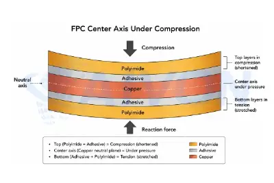
Copper lies farther from the neutral axis than the polyimide film. When a dynamic FPC bends, the outer surface is placed under tensile strain while the inner surface experiences compressive strain. Under comparable bend-radius and stack-up conditions, a thinner copper layer generally reduces the amount of conductor material exposed to high bending stress. This is why selecting the appropriate flexible PCB copper thickness is an important part of dynamic-flex design. Reducing copper from 35 µm to 18 µm can substantially lower conductor strain, although the actual strain reduction depends on the complete bend-zone construction and neutral-axis position. When repeated bending produces sufficiently high cyclic strain, plastic deformation and fatigue damage can accumulate in the copper, eventually initiating and propagating micro-cracks.
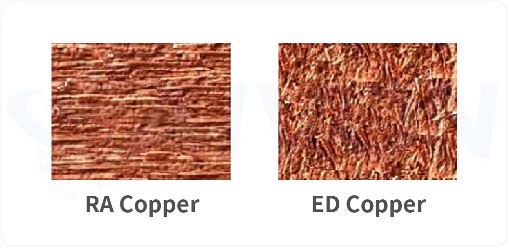
Rolled-annealed (RA) copper tolerates higher strain than electrodeposited (ED) copper because of its elongated grain structure. Even so, thinner RA copper is generally preferred for demanding dynamic-flex applications because it reduces bending strain. Industry data and accelerated testing consistently show that reducing copper from 35 µm to 18 µm or 12 µm can i significantly improve dynamic-flex life, depending on bend radius, copper type, and total stack thickness.
The failures are familiar: transverse cracks across traces, lifted pads at the edge of the bend zone, adhesive delamination between copper and polyimide, and coverlay wrinkling. These appear first in the highest-strain regions and then propagate. Static bend-to-install areas almost never need thinning because the board experiences only one or two cycles. Dynamic zones such as hinges, continuous motion joints, or catheter tips may require it. Secondary benefits appear during etching. Thinner copper produces a higher etch factor, more vertical sidewalls, and better width control. That is why the same fabricator that struggles to hold 75/75 µm on 35 µm copper can routinely deliver 40/40 µm or tighter once the copper is thinned to 12–18 µm.
FPC Copper Thinning Techniques
Four routes are used in production. Each has different process windows, cost, and design implications.
Starting with Thin RA Copper Foil
Starting with thinner RA foil is the cleanest method. Specifying 12 µm or 18 µm RA copper from the laminate supplier avoids any post-lamination chemistry and preserves the preferred grain orientation parallel to the bend axis. It is the preferred choice when the entire panel can accept the reduced thickness.
Uniform Chemical Copper Thinning
Panel-level chemical thinning reduces a thicker starting foil uniformly. After lamination or sometimes before patterning, the panel passes through a controlled micro-etch or half-etch bath until the residual copper reaches the target. Surface roughness increases modestly, so subsequent coverlay adhesion and any additional plating must be verified. Thickness uniformity across the panel is typically held within ±2–3 µm on well-controlled lines.
Selective Copper Thinning
Selective copper reduction protects static or high-current regions with dry film while etching only the dynamic zones. The sequence usually involves imaging, half-etch, strip, and optional re-plating if additional thickness is needed in the protected areas. Transition zones between thick and thin copper must be designed with gradual width or thickness changes; abrupt steps become stress concentrators. This approach is essential for mixed static/dynamic layouts.
Hybrid Thin-Copper and Selective Plating
Hybrid constructions begin with an ultra-thin seed layer or thin foil and build copper only where current or mechanical strength is required. Semi-additive or modified semi-additive processes fall into this category. They enable the finest geometries but add process steps and cost.
Process–design matching is critical. Uniform thinning or starting thin foil works for pure dynamic boards. Selective reduction or hybrid is mandatory when power planes or static connector regions must remain thicker. Artwork must be compensated for the final copper thickness; etch undercut changes with thickness, so the same line-width compensation used for 35 µm copper will be wrong for 12 µm copper. Coverlay openings and stiffener edges also interact with residual copper height—thinner copper reduces stress concentration at the coverlay edge but can lower peel strength if the surface is over-roughened.
|
Approach |
Best For |
Typical Residual Tolerance |
Relative Cost |
Fine-Line Advantage |
|---|---|---|---|---|
|
Start thin RA foil |
Uniform dynamic boards |
±2 µm |
Lowest |
High |
|
Panel chemical thinning |
Uniform reduction from thicker foil |
±2–3 µm |
Medium |
High |
|
Selective reduction |
Mixed static/dynamic |
±3 µm in thinned zones |
Higher |
High in thinned areas |
|
Hybrid thin-core + selective plate |
Extreme density + high current |
±2 µm |
Highest |
Highest |
How to Choose FPC Copper Thickness
Selecting the right FPC thickness is one of the highest-leverage decisions in flexible PCB design. Too thick and dynamic zones crack; too thin and resistance rises or impedance targets become difficult to hold. The goal is to match thickness to the mechanical and electrical demands of each region rather than applying a single value across the entire board.
Begin by mapping every dynamic flex zone against static or high-current areas. Record the expected bend radius and cycle count for the dynamic regions. Next determine the current-carrying needs and any controlled-impedance requirements. With those constraints clear, set the maximum allowable copper thickness for mechanical reliability. For aggressive dynamic flex this is commonly 18 µm or less of rolled-annealed copper.
Once the thickness limit is fixed, evaluate the resulting minimum flexible PCB trace width and space that the fabricator can hold. Then choose the practical thinning method: starting with thin foil, uniform chemical reduction, selective etching, or a hybrid approach. Finally confirm the fabricator's process capability, residual-thickness tolerance, and dynamic-flex test methods before releasing artwork.

Application patterns provide useful starting points. Wearables and foldable displays commonly use 12–18 µm rolled-annealed copper in dynamic flex zones. Medical devices that require extreme flexibility, such as certain catheters, often adopt even thinner copper with careful current budgeting. Automotive hinges may keep 18 µm copper for vibration durability while thinning only the pure dynamic segments.
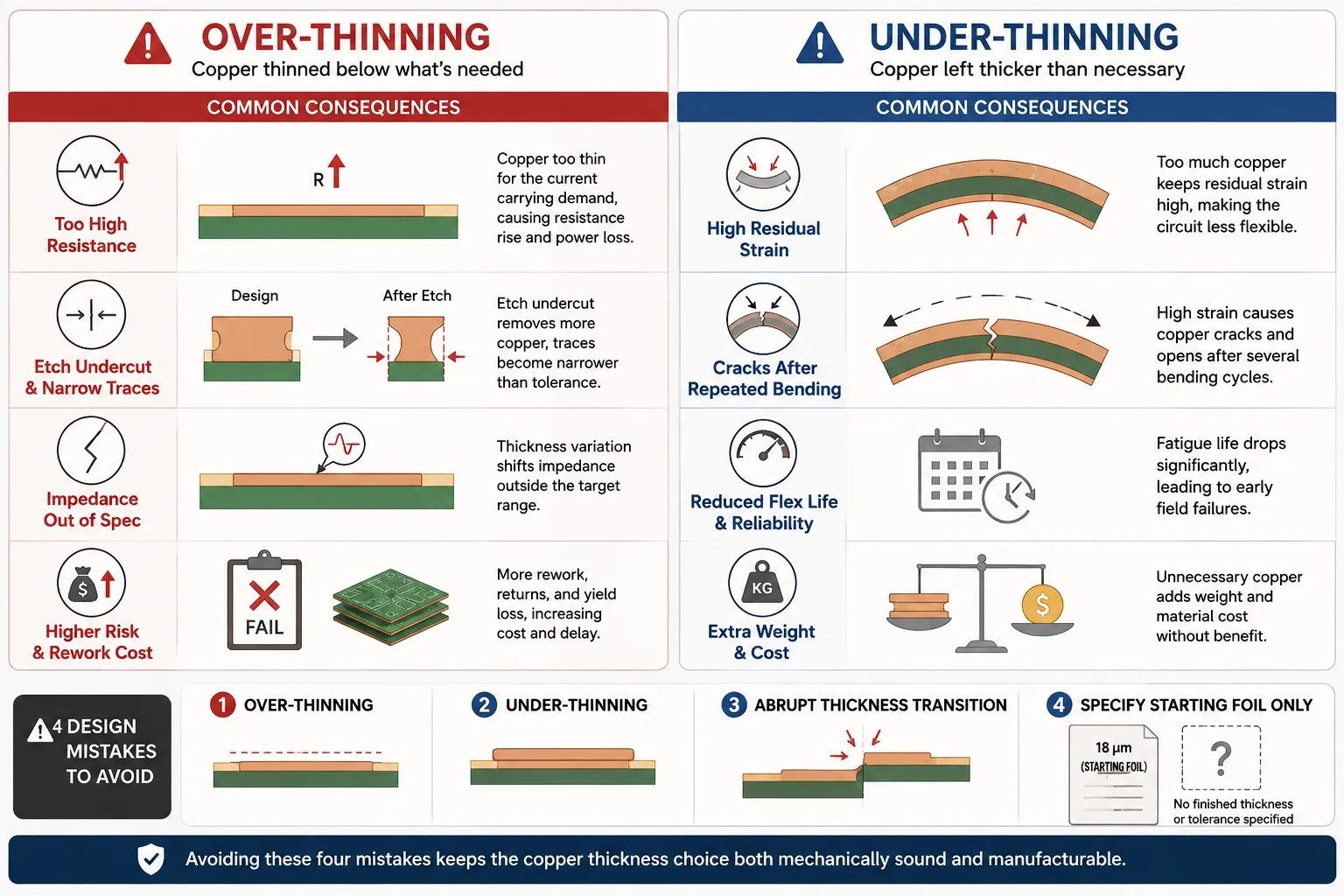
When choosing FPC copper thickness, several practical mistakes can undermine the entire decision. Over-thinning is one of the most common. Designers sometimes push copper below the minimum needed for current or impedance, only to discover that resistance rises too high or etch undercut narrows the traces beyond tolerance. Under-thinning creates the opposite problem: residual strain remains high and cracks still appear after repeated bending. Abrupt thickness transitions between static and dynamic zones are another frequent source of failure; without gradual fillets the stress concentrates exactly where the copper changes height. Finally, many drawings still specify only the starting foil weight. Without a clear finished copper thickness and tolerance, the fabricator cannot control the process tightly enough to protect either flex life or impedance. Avoiding these four mistakes keeps the thickness choice both mechanically sound and manufacturable.
How Copper Thickness Affects FPC Trace Width and Impedance
Flexible PCB copper thickness directly influences both the smallest manufacturable trace width and the characteristic impedance of flexible circuits. Thinner copper produces a higher etch factor and less undercut, so the practical limit of flexible PCB trace width and space improves.
In impedance control the same reduction changes the geometry that the field solver sees. Lower copper height reduces the aspect ratio of the trace and slightly increases the effective dielectric height to the reference plane. To hold a target of 50 Ω single-ended or 90–100 Ω differential, the designer must either widen the trace or increase dielectric thickness. In practice this often means that thinner copper still permits narrower traces than the original thick-copper design while meeting the same impedance, provided etch compensation is recalculated for the new thickness.
Tolerance stack-up becomes tighter with thin copper. Variation in residual thickness after thinning, etch undercut, and dielectric thickness all contribute to impedance spread. Specifying finished copper thickness and tolerance rather than starting foil weight is therefore essential for consistent results.
FPC Copper Thinning Design Considerations
Successful copper thinning begins with a clear zone map that separates dynamic flex regions from static or high-current areas. Only the dynamic zones should be thinned; static regions can retain thicker copper when current capacity or mechanical robustness is required.
Artwork must be compensated for the final copper thickness because etch undercut changes with height. The compensation values used for 35 µm copper will under- or over-correct once the copper is reduced to 12–18 µm. Transition zones between thick and thin copper need gradual width or thickness changes; abrupt steps become stress concentrators and can initiate cracks.
Coverlay openings, stiffener edges, and adhesive systems also interact with residual copper height. Thinner copper reduces stress concentration at the coverlay edge but can lower peel strength if the surface is over-roughened during chemical thinning. Current-carrying capacity must still be verified after thinning; wider traces or additional copper in non-flex areas may be needed to keep resistance and temperature rise within limits.
Finally, the fabrication drawing should call out finished copper thickness and tolerance in each zone rather than starting foil weight. This single clarification improves both process control and impedance.
Manufacturing Tolerances and Quality Control
Thinner copper changes etch dynamics in the designer's favor. Lower aspect ratios reduce undercut, so the practical limit of flexible PCB trace width and space improves. Typical industry capability after controlled thinning is 25/25 µm or 20/20 µm on 12–18 µm copper; advanced lines reach finer geometries when starting foil quality, etch chemistry stability, and post-thinning AOI are tightly controlled.

Mixed-thickness boards require special attention to transition zones. Fabricators inspect residual copper by cross-section or non-destructive methods and run dynamic flex testing plus thermal cycling to validate the design. Designers must supply zone maps, finished copper targets, impedance requirements, and flex-life expectations so the FPC manufacturer can confirm manufacturability.
AIVON routinely processes base copper of 12 µm, 18 µm and 35 µm on flexible constructions and supports fine-line geometries consistent with these thicknesses while performing dynamic flex testing as part of process validation. That capability level is representative of fabricators that have invested in controlled thinning, residual-thickness measurement, and reliability testing.
Process controls that matter most are starting foil quality, etch bath stability, inspection of residual thickness before coverlay, and AOI after thinning. Without these, the theoretical fine-line benefit disappears.
Conclusion
FPC copper thinning is an effective way to balance flexibility, fine-line capability, and electrical performance in flexible circuit design. However, the correct copper thickness depends on the complete application rather than one universal value.
The terms flexible PCB copper thickness, flex PCB thickness, and overall flexible PCB thickness should be considered together. For example, a 0.30mm FPC may be suitable for a design that needs additional mechanical support, but its performance will depend on how the total thickness is distributed across the substrate, copper, coverlay, adhesive, and stiffeners.
By selecting the right thinning method and confirming the final stack-up with the manufacturer, designers can achieve a more reliable and manufacturable flexible PCB.
FAQs
Q1: What finished copper thickness is typically recommended for dynamic flex zones in FPC?
A1: Most demanding dynamic applications use 12–18 µm rolled-annealed copper. Values below 12 µm can further improve flex life but require careful current-carrying and impedance considerations, along with tighter process control.
Q2: Can controlled impedance be maintained after selective copper thinning?
A2: Yes. Simulate the stack-up using the final copper thickness for each zone, apply the correct etch compensation, and keep transition regions outside critical impedance-controlled nets. Specifying the finished copper thickness and its tolerance is essential for maintaining impedance consistency.
Q3: Is selective copper thinning more expensive than starting with thinner foil?
A3: Usually yes. Selective masking, additional processing steps, and potentially lower yield increase both cost and lead time. Starting with thinner RA copper foil is generally preferred when the entire circuit can accept the reduced copper thickness.
Q4: What reliability tests should be performed after copper thinning in dynamic areas?
A4: Perform dynamic flex cycling to the required cycle count at the specified bend radius, followed by continuity and insulation-resistance testing. Thermal cycling and cross-section inspection of the thinned regions and transition zones should also be performed to verify process integrity and long-term reliability.
Q5: How should finished copper thickness versus starting foil weight be specified on fabrication drawings?
A5: Always specify the finished copper thickness and tolerance, together with a zone map when selective thinning is required. Starting foil weight alone is insufficient for controlling the finished thickness, process consistency, and impedance yield.
Q6: What is the typical FPC thickness?
A6: There is no single standard FPC thickness for every flexible PCB. The finished thickness depends on the polyimide substrate, copper layers, coverlay, adhesive, stiffeners, and overall stack-up. Thin constructions are often used for dynamic bending and compact packaging, while thicker constructions may be preferred for mechanical support, connector areas, or higher-current sections. The required thickness should be selected according to the bend radius, electrical requirements, available space, and manufacturing capability.
Q7: How does flexible PCB copper thickness affect FPC performance?
A7: Flexible PCB copper thickness affects flexibility, resistance, current capacity, trace geometry, and impedance. Thinner copper can reduce bending strain and support fine-line routing. However, it may also increase resistance and reduce current-carrying capability. Thicker copper may be more suitable for static or high-current areas, but it can increase stiffness and bending strain in dynamic zones. The best choice depends on the complete FPC construction and application requirements.
Q8: What is the difference between FPC thickness and copper thickness?
A8: FPC thickness refers to the overall finished thickness of the flexible circuit. Copper thickness refers only to the copper layer. Overall FPC thickness may include the polyimide substrate, copper, coverlay, adhesive, stiffeners, and other layers. Therefore, two FPCs with the same finished thickness may have different copper thicknesses and different bending performance. Both specifications should be clearly defined in the fabrication drawing.
Q9: Is a 0.30 mm FPC suitable for flexible applications?
A9: A 0.30 mm FPC may be suitable for applications that need more mechanical support or a thicker flexible construction. However, finished thickness alone does not determine whether the circuit is suitable for bending. The designer should also evaluate copper thickness, polyimide thickness, coverlay and adhesive structure, stiffener placement, bend radius, bending frequency, static or dynamic use, and connector and component locations. A 0.30 mm FPC may work well in a static bend or supported routing area, but a continuously moving section may require a thinner and more carefully designed construction.






