










In HDI layouts the distance between vias is treated as a simple density rule. The CAD system accepts the number, the designer moves on, and the board goes to fabrication. The problems appear later—during laser drilling, during plating, or months later in reliability testing. When HDI via to via spacing drops below the process window, the intervening dielectric is no longer a reliable insulator. It becomes a thin web that can crack, trap chemistry, or allow copper to bridge.
The failure is rarely a clean short at electrical test. More often it is intermittent leakage, progressive insulation resistance drop, or cracks that only open after thermal cycling. The root cause is almost always the same: the designed spacing did not leave enough solid dielectric after laser ablation, registration tolerance, and plating growth were accounted for.
Laser Drilling and the Heat-Affected Zone Between Vias
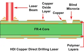
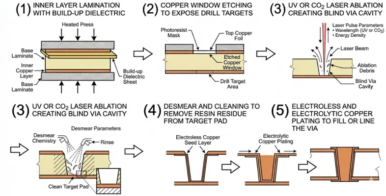
Laser microvia formation removes dielectric by ablation. Each pulse leaves a heat-affected zone around the hole wall. When two vias are placed close enough that their heat-affected zones overlap, the dielectric between them is partially degraded even before the second hole is fully formed. The result is a weaker web of material that is more susceptible to cracking during subsequent lamination or thermal stress.
On CO2 laser systems the effect is more pronounced because of the larger thermal footprint. UV lasers produce a narrower affected zone, but the principle remains. If the edge-to-edge distance between two microvias approaches or falls below the combined heat-affected width, the intervening dielectric loses integrity. In extreme cases the laser can break through the web entirely, creating an irregular double hole or a slot instead of two discrete vias.
The problem is worse in sequential build-up constructions. Each new dielectric layer inherits any weakness from the vias below. Closely spaced stacked microvias amplify the thermal damage through the column.
Copper Plating Behavior in Tight Via Clusters
Once the holes exist, electroless and electrolytic copper must coat the walls uniformly. When vias sit close together the local current density and solution flow change. Chemistry can become depleted or trapped in the narrow dielectric channel between the holes. The result is thin copper on the facing walls, seams, or voids that later act as stress risers.
In filled microvia processes the risk shifts to bridging. If the remaining dielectric web is thin and the plating process has any over-growth or nodule formation, copper can grow across the gap and create a short between adjacent vias. This is more common on outer HDI layers where the plating thickness is higher and the process window is already tight.
Desmear chemistry also suffers. The narrow channel between close vias does not exchange fluid efficiently. Residues remain, interfere with electroless adhesion, and create the classic "weak wall" that fails under thermal cycling.
Registration Tolerance Consumes Designed Spacing
Laser positioning accuracy on modern HDI lines is typically held to ±25–50 µm. That number is the best-case capability under controlled conditions. Real panels see additional variation from dielectric thickness, copper foil movement, and the cumulative registration of previous layers. When two vias are designed with only 0.20 mm center-to-center spacing, a 40 µm shift on each via can reduce the remaining dielectric web to nearly zero.
The same tolerance stack applies when mechanical vias and laser microvias share the same area. The mechanical drill has its own positional tolerance; the laser has another. The effective HDI via to via spacing that remains after both processes can be substantially smaller than the CAD dimension.
CAM review routinely flags clusters where the designed spacing sits inside the combined process tolerance. The question is not whether the nominal number meets the rule book. The question is whether the worst-case remaining web of dielectric is still thick enough to survive plating and field life.
Reliability Consequences of Insufficient Dielectric Web
Even if the vias survive fabrication without shorts, a thin dielectric bridge between them is a long-term liability. Under thermal cycling the CTE mismatch between copper and dielectric concentrates stress at the narrowest point. Cracks initiate in the web and propagate, eventually linking the two plated walls or creating paths for conductive anodic filament growth.
Insulation resistance between the vias degrades over time, especially in humid environments. The failure may not appear at initial electrical test. It appears after multiple reflow cycles or after the product has been in the field. Boards with dense via clusters in high-reliability applications are particularly exposed to this mechanism.
Stacked microvia columns that are placed too close to neighboring columns compound the problem. Each interface in the stack inherits any weakness in the dielectric, and the entire column becomes a stress concentrator.
Practical Spacing Values That Survive Production
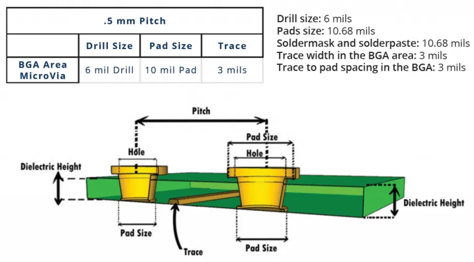
For most production HDI the safe center-to-center spacing between laser microvias starts at 0.30–0.35 mm when the via diameter is 75–100 µm. That range leaves a usable dielectric web after laser heat-affected zones and typical registration tolerances are subtracted. Edge-to-edge clearance should remain at least 0.10–0.15 mm in the worst-case registered position.
Tighter spacing is possible on advanced lines with UV lasers and demonstrated process control, but it must be treated as a special process, not a default rule. Going below 0.25 mm center-to-center on commercial HDI constructions routinely produces higher scrap at plating or reliability failures later.
When density forces closer placement, the preferred solution is to stagger the vias across layers rather than pack them on the same layer. Staggering restores dielectric thickness between any two plated features and reduces the cumulative registration risk. Stacked vias should be kept farther apart than staggered ones for the same reason.
Design Rules That Include Process Reality
The CAD rule for HDI via to via spacing should be set larger than the fab's published minimum by the amount of expected registration variation plus a small reliability margin. A common practical approach is to take the fab's capability number and add 0.05 mm. That extra distance absorbs normal process drift across a production lot.
Rules should also distinguish between same-layer spacing and spacing between vias on adjacent layers in a staggered pattern. The dielectric thickness between layers provides additional isolation that same-layer spacing does not. Treating both cases with the same number either wastes density or creates hidden risk.
Finally, document the measurement method. Center-to-center is unambiguous. Edge-to-edge depends on whether the measurement is taken from the finished hole wall or the outer edge of the capture pad. CAM software will use its own definition; matching it in the design notes prevents unnecessary engineering queries.
HDI via to via spacing is not a theoretical minimum that can be pushed until the CAD system complains. It is the thickness of solid dielectric that remains after laser ablation, registration, and plating. When that thickness becomes too small, the board may still leave the fab, but its long-term insulation integrity is already compromised. The designs that run cleanly are the ones that treated the intervening dielectric as a structural element, not an empty keep-out.






