










Flexible PCBs are designed to bend, fold, or conform to a product's mechanical structure, but flexibility does not mean they can be bent to any radius. The flex PCB bend radius is one of the most important mechanical design factors because a bend that is too tight can increase strain in the copper, coverlay, and dielectric layers.
The required FPC bend radius depends on the finished thickness, layer count, copper type, stack-up, and whether the circuit is used for static or dynamic bending. A circuit that is formed once during assembly has different requirements from an FPC that bends repeatedly during operation.
Good flexible PCB bending design also requires more than selecting a suitable radius. Sharp corners, vias, pads, trace transitions, and stiffener edges can create local stress concentrations even when the overall bend radius appears acceptable.
Highlights
• Static applications typically allow 6× total thickness; dynamic applications often need 100× or more, with single-layer RA copper preferred.
• Sharp corners, via edges, and stiffener transitions create local stress peaks even when the nominal radius is correct.
• Teardrops, gradual tapers, rounded outlines, and proper stiffener clearance form the core of reliable Flexible PCB stress relief.
In this guide you will see material-based radius tables, a simple calculation method, the exact layout zones that cause most cracks, proven stress-relief geometries, stiffener placement rules, and a ready-to-use design checklist you can apply on the next board.
What is FPC Bend Radius and How Does It Affect FPC Stress?
The FPC bend radius is the inner radius of the curved section of the flexible circuit. It is measured from the innermost surface of the bend. Two distinct regimes exist. Static bends occur once during assembly and remain fixed. Dynamic bends cycle repeatedly during product life—hinges in foldables, printer heads, or robotic joints.
When a flex circuit bends, the outer copper experiences tensile stress while the inner copper sees compression. Shear forces appear at the copper–adhesive–coverlay interfaces. If the radius is too small relative to stack thickness, the copper exceeds its fatigue limit and cracks. Adhesive layers separate and coverlay ruptures. Even a correctly sized nominal radius can still fail if local features create stress concentrations: a sharp 90° outline corner, a via sitting inside the bend zone, or an abrupt stiffener edge all act as crack initiation sites.
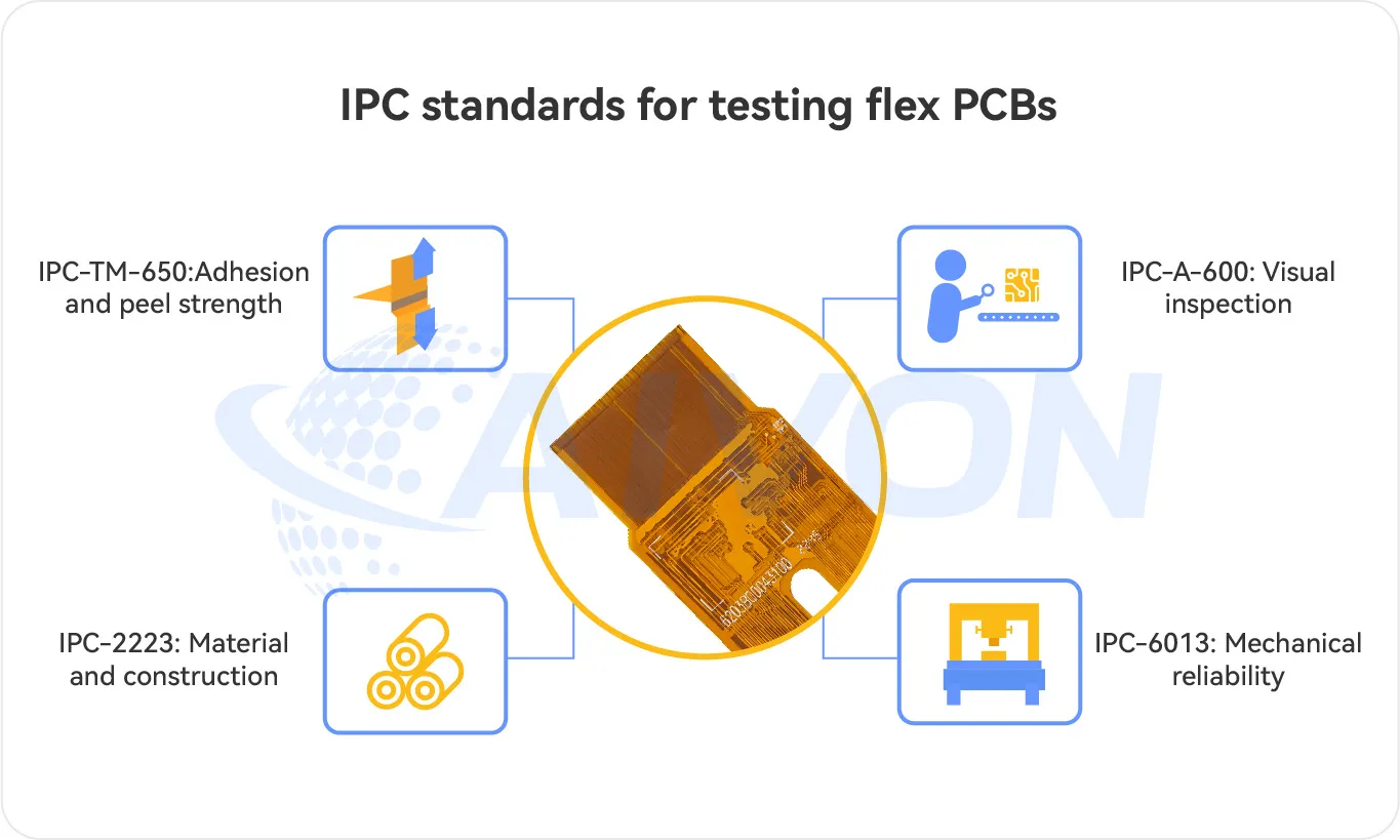
IPC-2223 and IPC-6013 provide the baseline most OEMs and fabricators reference. They supply multiplier guidelines rather than absolute numbers, because allowable radius depends on total thickness, copper type, layer count, and expected cycle life. Designers who treat the standard as a starting point and then add layout-level stress relief achieve far higher first-pass yield.
Why Bend Radius Matters in Flexible PCB Bending
During flexible PCB bending, the outer side of the circuit is placed under tensile strain while the inner side experiences compression. Copper located farther from the neutral axis generally experiences greater strain.
A suitable bend radius helps distribute this strain over the bend area. A poorly selected radius can concentrate stress in the copper or at geometric features such as vias, pads, trace transitions, and stiffener edges.
FPC Bend Radius Guidelines by Thickness and Layer Count
Total finished thickness is the primary driver. Copper weight, number of copper layers, coverlay thickness, and adhesive versus adhesiveless construction further adjust the multiplier. Rolled-annealed (RA) copper tolerates repeated flexing better than electrodeposited (ED) copper because of its elongated grain structure; use RA for any dynamic application.
Typical industry practice synthesized from IPC-2223 guidance and production experience:
|
Construction |
Static |
Dynamic |
Notes |
|---|---|---|---|
|
Single-sided |
6× total flex thickness |
100× total flex thickness |
Preferred for high-cycle dynamic |
|
Double-sided |
10× total flex thickness |
150× total flex thickness |
Stagger traces; keep copper near neutral axis |
|
Multilayer flex |
12× total flex thickness |
Generally not recommended |
Consider air-gap construction or move to rigid-flex |
For a 0.1 mm single-sided PI circuit the static radius might be 0.6 mm while a dynamic requirement can jump to 10 mm. Heavier copper or extra coverlay layers push the number higher. When the calculated radius becomes impractical, switch to rigid-flex so the bend occurs only in a controlled single- or double-layer flex zone.
Copper annealing and grain orientation also matter. RA copper can be specified with the rolling direction parallel or perpendicular to the bend axis; many high-cycle designs place the long grain direction across the bend for maximum fatigue resistance.
How to Calculate the Minimum Bend Radius?
The minimum bend radius is one of the most critical numbers in any flexible circuit layout. Get it wrong and the copper will fatigue, the coverlay will delaminate, or the traces will crack.
For most dynamic flexible printed circuits, the simple industry starting point is:
Minimum bend radius = 100 × finished thickness of the flex circuit.
Finished thickness means the total thickness of the completed flexible section after all layers are laminated, including polyimide, copper, adhesives, and coverlay.
Example: A dynamic flex circuit with a finished thickness of 0.15 mm requires a minimum bend radius of 15 mm, which equals a minimum bend diameter of 30 mm. This ratio keeps the copper strain low enough for reliable cycle life under normal conditions.
For static applications the multiplier is much smaller, typically in the 6× range depending on layer count, because the circuit only needs to survive a single forming operation. Always confirm the exact static multiplier with your fabricator's stack-up data, because even static designs can fail if the radius is pushed too tight during assembly.
In real designs the exact multiplier also changes with the number of layers and how often the circuit will bend. Many fabricators therefore use a more detailed set of ratios that distinguish between stable, semi-dynamic, and fully dynamic applications. The table below shows typical values for common constructions:
|
Layers |
Example Thickness |
Stable |
Semi-Dynamic |
Dynamic |
|---|---|---|---|---|
|
1 Layer |
90 μm |
10:1 → 0.9 mm |
20:1 → 1.8 mm |
100:1 → 9 mm |
|
2 Layers |
190 μm |
10:1 → 1.9 mm |
20:1 → 3.8 mm |
150:1 → 29 mm |
|
4 Layers |
290 μm |
20:1 → 5.8 mm |
50:1 → 15 mm |
Not recommended |
These ratios are practical guidelines, not absolute limits. Always confirm the final number with your fabricator's stack-up data or request a sample flex-life test, especially for multilayer or high-reliability flexible circuit board design. When the calculated radius becomes too large for the mechanical envelope, the usual solutions are to thin the stack, move to a single-layer design, or convert the bend area to rigid-flex.
Step-by-Step Calculation
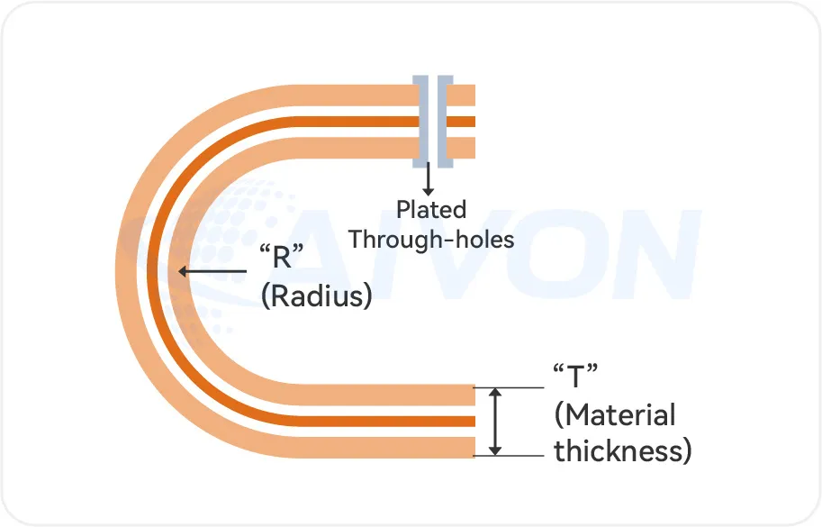
1. Measure the total finished thickness (t):
Add up every layer in the flexible section: copper, dielectric, adhesive, and coverlay. Use the final laminated thickness, not the individual material thicknesses.
2. Select the Bending Factor (N):
Choose the factor according to the number of layers and static vs dynamic bend radius. Single-layer circuits usually allow a smaller factor than double-layer or multilayer circuits.
3. Calculate the flex PCB minimum bend radius:
Use the formula: R = t × N.
Example:
A double-layer flex circuit has a total finished thickness of 0.2 mm.
Using a common factor of N = 12 for this construction:
R = 0.2 × 12 = 2.4 mm
The minimum bend radius for this board is therefore 2.4 mm.
When the calculated radius becomes impractical for the mechanical design, options include thinning the stack, moving to a single-layer design with the copper on the neutral axis, or converting the critical bend zone to a rigid-flex construction so the flex section can remain thin and simple.
Rule-of-thumb values are useful for early layout, but they are not a substitute for validation. High-reliability or high-cycle applications should always be confirmed with finite-element analysis or physical bend testing using the exact materials and stack-up that will go into production.
How Bend Radius Affects FPC Bending Strain
When a flexible circuit bends, the copper and dielectric layers experience mechanical strain. The size of the bend radius directly controls how large that strain becomes.
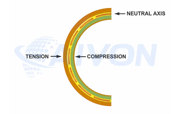
During flexible PCB bending, the outer surface of the circuit is placed under tension while the inner surface is compressed. On the inner side it is compressed. The center of the stack, the neutral axis, sees almost no strain if the construction is balanced. The farther a copper layer sits from the neutral axis, and the tighter the radius, the higher the strain becomes.
A simple approximation for the maximum strain is:
Strain ≈ t / (2R)
where
t = total finished thickness of the flex section
R = bend radius
This relationship explains why the industry uses large multipliers such as 100× thickness for dynamic applications. A larger radius keeps the strain low enough that the copper stays within its elastic range and does not accumulate fatigue damage over thousands of cycles. A smaller radius pushes the copper past its fatigue limit, leading to microscopic cracks that eventually open into open circuits.
The same principle applies to the adhesive and coverlay layers. Excessive strain can cause them to delaminate or tear even if the copper itself survives. That is why designers not only choose a large enough radius but also try to keep the copper close to the neutral axis and avoid any features that create local strain peaks.
Common Stress Concentration Areas in FPC Bending
Even when the overall radius meets the table, cracks still start at predictable locations. The highest-risk zones are:
● Sharp 90° corners in the outline or copper pattern
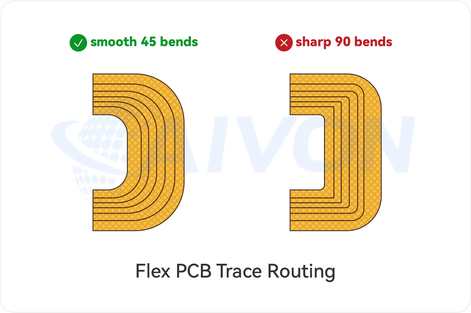
● Transition zones between rigid and flex sections
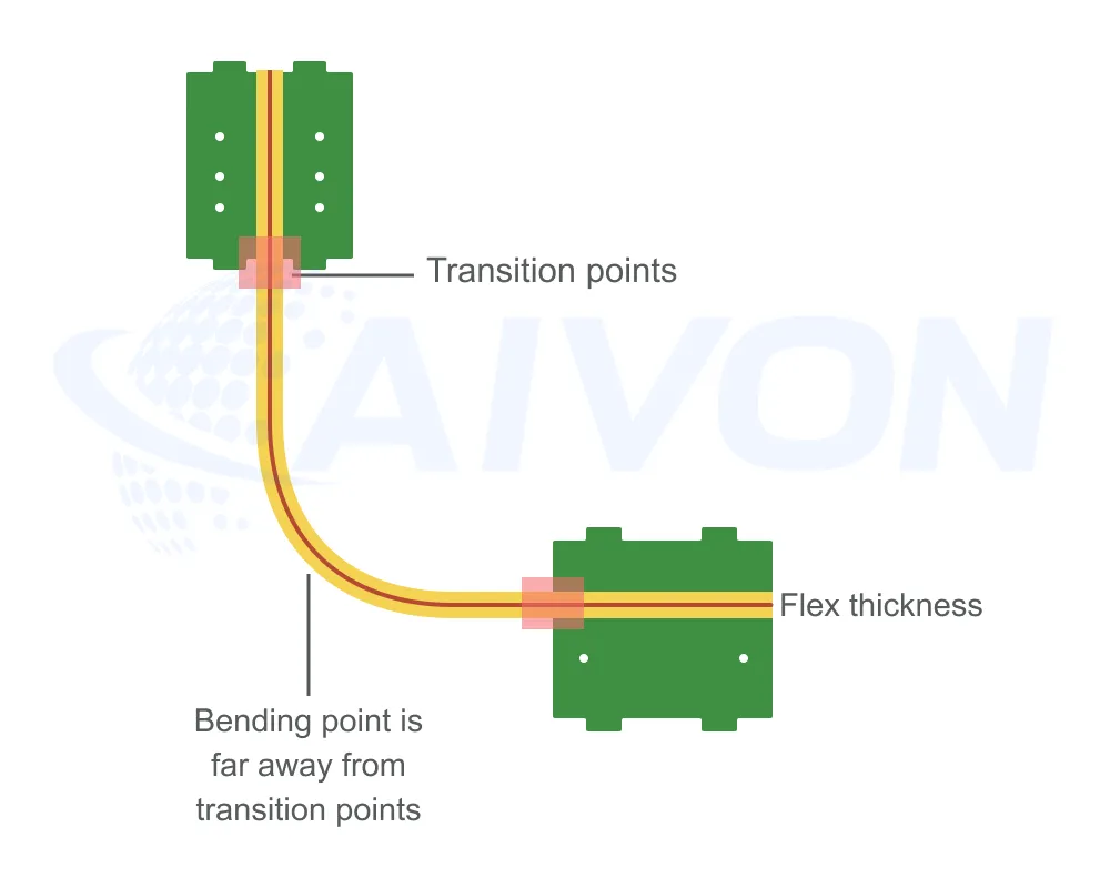
● Via and pad edges that sit inside or near the bend area
● Stiffener edges that create abrupt thickness transitions and stress concentrations
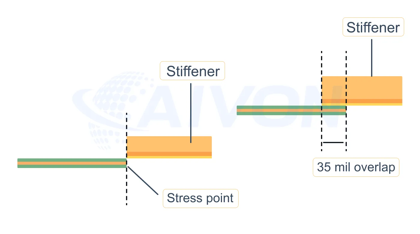
● Trace neck-downs or sudden width changes inside the bend region
These features amplify local strain. Reliability testing routinely shows cracks originating at a via knee or a square outline corner and propagating across the copper. Keeping every plated hole and component pad outside the active bend zone is the single most effective layout rule. Maintain at least 0.5–1 mm clearance between any via and the bend line.
FPC Stress Relief Design Techniques
Three simple geometry changes can dramatically lower the stress that causes copper cracks.
Teardrop pads and vias
Make the trace gradually wider as it enters a pad or via. A good teardrop is about 1.2 to 1.5 times the trace width and uses a smooth curve instead of a sharp angle. Put teardrops on every pad and via that sits near a bend or a rigid-to-flex transition. They remove the sharp corner where cracks almost always start.

Tapered trace transitions
When a trace enters the bend area, change its width slowly. Aim for a length-to-width ratio of at least 3:1 and keep the angle no steeper than 45°. This spreads the strain evenly instead of concentrating it at one point.
Rounded corners and cut-outs
Give every outline corner and internal cut-out a minimum radius of 1.5 mm. Sharp corners act like stress magnets and can start tears. If you need a relief slot, end it with a round hole at least 1.5 mm in diameter.
A few extra habits also help:
● On double-sided flex, stagger the traces so they do not sit directly on top of each other.
● Keep copper density fairly even across the bend zone.
● Route traces at right angles to the bend line whenever possible.
● Replace solid copper pours with cross-hatch patterns, or remove them completely in dynamic areas.
● Prefer gentle curves over sharp angles in the routing.
These features work best when they are combined with a properly sized bend radius. A correct radius plus teardrops and rounded corners routinely gives much longer flex life than the same board without them.
FPC Cable Bend Radius Considerations
The term FPC cable bend radius is often used when a flexible circuit is functioning as a cable or interconnect between two assemblies.
The same mechanical principles apply, but the cable's movement pattern becomes especially important.
FPC Cable Bend Radius vs PCB Bend Radius
An FPC used as a cable may experience continuous movement, repeated folding, or controlled installation bends.
Therefore, the required FPC cable bend radius depends not only on the board construction but also on how the cable moves inside the final product.
A cable that is installed once may tolerate a different radius from one that moves continuously during operation.
Why Stiffener Edges Create Stress Concentration
A FPC stiffener is added to make part of the flexible circuit rigid, usually under connectors or components. While this is useful, the edge of the stiffener creates a sudden change in thickness and stiffness.
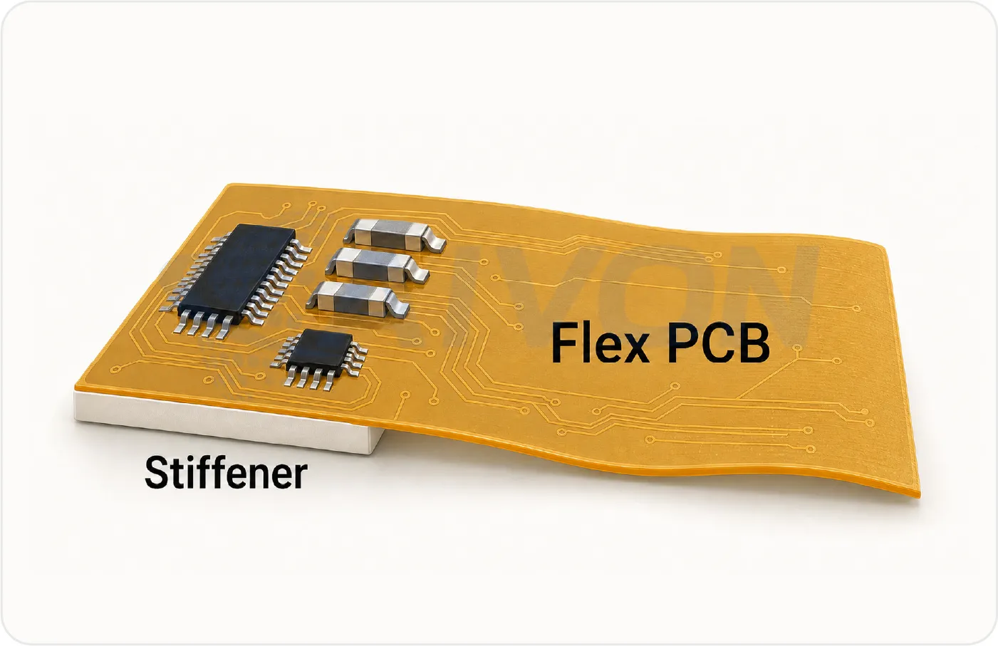
When the circuit bends, the flexible area can curve freely, but the stiffened area cannot. The transition happens abruptly at the stiffener edge. This edge acts like a hard hinge or fulcrum. All the bending strain that should be spread over a larger area is forced into a very narrow zone right at the edge.
As a result, the copper traces, adhesive, and coverlay experience a sharp local peak in stress. Even if the overall bend radius meets the recommended value, cracks often start exactly at this transition line. Over repeated cycles the damage grows and can lead to open circuits or delamination.
This is why proper stiffener placement is critical. The edge must sit far enough away from the intended bend zone so the thickness change does not become a stress riser. Understanding the flexible PCB with stiffener can also help ensure proper dimensional stability and placement during manufacturing. Using a tapered or stepped edge, or multiple thin polyimide layers instead of one thick steel stiffener, also helps distribute the strain more gradually.
Flexible PCB Bend Radius Design Checklist
Follow this sequence on every new layout:
1. Define the application (static install versus dynamic cycles plus expected life).
2. Select base material and construction from the bend-radius table.
3. Calculate or confirm the minimum radius and add margin.
4. Map every stress-concentration zone and apply teardrop, taper, and radius features.
5. Locate and size stiffeners with proper edge clearance.
6. Review stack-up thickness consistency and copper balance across the bend.
Trade-offs are straightforward. Larger radius and single-layer RA copper raise reliability but may increase size or cost. Multilayer constructions reduce layer count elsewhere yet demand larger radii or air-gap construction. A quick go/no-go checklist before Gerber release:
● Radius meets or exceeds table value for the application
● No vias or pads inside the bend zone
● All outline corners ≥ 1.5 mm radius
● Teardrops present on every critical pad/via
● Stiffener edges clear of the bend by ≥ 1.5 mm
● Traces perpendicular and staggered
● Copper type and coverlay match static or dynamic needs
Conclusion
Getting the flex bend radius right and adding proper stress-relief features is what separates a flexible circuit that lasts from one that cracks in the field.
Start by confirming whether the application is static or dynamic, then apply the correct multiplier to the finished thickness. Next, remove every local stress point—sharp corners, vias inside the bend zone, and abrupt width changes. Finish by placing stiffeners so they guide the bend instead of creating a new weak spot.
The rules, tables, and checklist in this article give design and manufacturing teams a clear, practical way to raise reliability without over-complicating the board. Use them on the next layout, and always double-check the final stack-up and bend life with your fabricator.
Beyond bend radius and stress relief, good flexible-circuit design also depends on choosing the right copper type, routing traces perpendicular to the bend, and keeping the overall stack-up as thin and balanced as possible. When these elements work together, the circuit becomes both more reliable and easier to manufacture.
FAQs
Q1: How does dynamic bend radius differ from static bend radius for flexible PCBs?
A1: Static applications can generally use tighter bend radii because the circuit is bent only occasionally or during installation. Dynamic applications require larger bend radii and typically use RA copper to keep cyclic strain within an acceptable fatigue range over thousands or millions of bending cycles.
Q2: Where should steel or PI stiffeners be placed relative to the bend area?
A2: Keep the stiffener edge at least 1.5–2.5 mm outside the active bend zone so the edge does not act as a fulcrum and create a stress concentration. For reliable bonding, the stiffener should typically overlap the coverlay by approximately 0.75 mm, subject to the fabricator's design rules.
Q3: Why do teardrop pads and tapered traces improve FPC reliability?
A3: Teardrop pads and tapered traces reduce sharp re-entrant corners and abrupt changes in copper geometry that can concentrate mechanical stress. These smoother transitions distribute strain more evenly and reduce the risk of crack initiation at pads, vias, and trace transitions near bend areas.
Q4: Can I use a smaller bend radius if I increase copper thickness?
A4: No. Increasing copper thickness generally increases circuit stiffness and bending strain, so the required bend radius typically becomes larger rather than smaller. Thinner copper and adhesiveless constructions can generally support tighter bends when the overall stack-up and application requirements are properly controlled.
Q5: Does IPC-2223 give exact bend-radius numbers or only guidelines?
A5: IPC-2223 provides design guidance and multiplier-based recommendations that account for factors such as layer count and static versus dynamic flexing. Exact bend-radius requirements still depend on total circuit thickness, copper type, temperature, and required cycle life. Additional design margin and physical validation testing are often recommended for demanding applications.
Q6: What is the minimum bend radius for a flex PCB?
A6: The minimum flex PCB bend radius depends on the finished thickness, layer count, copper construction, materials, and whether the FPC is used for static or dynamic bending. Thinner and simpler constructions can generally support tighter bends, while dynamic applications usually require a larger radius.
Q7: How do you calculate FPC bend radius?
A7: A common starting formula is R = t × N, where R is the bend radius, t is the finished thickness of the flexible section, and N is a bend-radius factor selected according to the construction and application. The factor is not universal, so the calculated value should be checked against the fabricator's recommendations.
Q8: How does FPC thickness affect bend radius?
A8: A thicker FPC generally requires a larger bend radius because more material is placed between the inner and outer surfaces of the bend. When a design requires a tight bend, reducing the thickness of the active flex section can help reduce the required radius.
Q9: Can a flex PCB bend too far?
A9: Yes. Bending an FPC beyond its suitable mechanical range can cause copper cracking, coverlay damage, delamination, or other reliability problems. The risk increases when the bend is tight, repeated, or combined with stress concentrations such as vias, sharp corners, or stiffener edges.
Q10: What is an FPC cable bend radius?
A10: The FPC cable bend radius is the radius within which an FPC used as a cable can bend without creating excessive mechanical stress. The appropriate value depends on the cable's thickness, layer structure, copper construction, reinforcement, and whether the cable is static or dynamically moving.
Q11: Can I use the same bend radius for static and dynamic FPCs?
A11: Not necessarily. Dynamic applications normally require a more conservative radius because the circuit must withstand repeated mechanical movement. A radius that is acceptable for a static installation may not provide sufficient margin for a continuously flexing application.
Q12: Does copper thickness affect FPC bend radius?
A12: Yes. Thicker copper generally increases stiffness and can increase the required bend radius, particularly in applications involving repeated movement. Copper type also matters. For dynamic applications, the copper construction should be selected together with the complete FPC stack-up and expected bending conditions.






