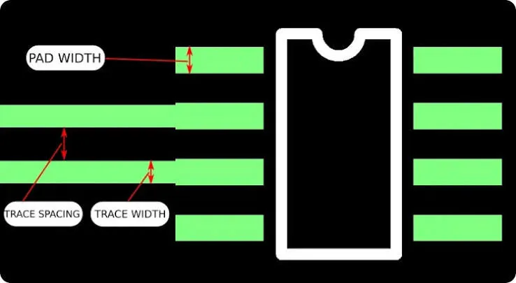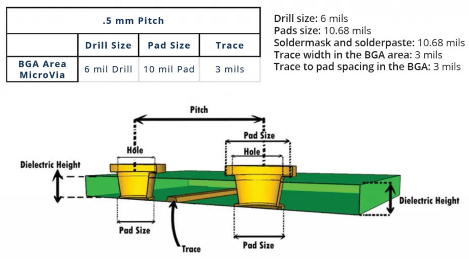







In HDI work the most common clearance violation I still see is not trace-to-trace. It is pad-to-trace. Designers push the copper of a fan-out trace or a dog-bone right up against a BGA or QFN pad because the routing channel is tight and the tool allows it. The layout looks clean. The DRC is green. Then the board hits the fab and the yield drops.
The root cause is almost always the same: the designed HDI pad to trace spacing did not leave enough margin for etch undercut plus solder-mask registration. Those two process realities turn a 3 mil gap into something that either shorts during etch or leaves no reliable dam under the mask.
How Etch Undercut Eats the Designed Clearance
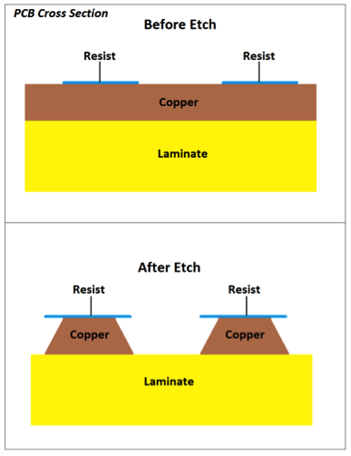
Subtractive etching is still the workhorse process for most HDI outer layers. Copper etches sideways as well as down. The undercut on ½ oz foil is typically 8–15 µm per side; on 1 oz it climbs higher. That means a 75 µm designed gap can finish closer to 50 µm or less once the resist is stripped.
When the gap is already at the edge of the process window, residual copper bridges form in the dense areas. AOI catches some of them. Electrical test catches the rest. The ones that slip through become field failures later.
Thinner starting foil helps. That is why most HDI shops push ⅓ oz or ½ oz on the outer layers when the designer is targeting 50–75 µm features. Even then the etch factor is never perfect. Isolated traces etch faster than dense ones. A pad sitting next to a long parallel trace sees more undercut on the trace side than on the open side. The asymmetry is real and it shows up in impedance and in isolation resistance.
Solder Mask Dam Collapse Between Pad and Trace
Even if the copper survives etch, the mask still has to isolate the pad from the nearby trace. Standard liquid photoimageable mask needs a minimum web of roughly 75–100 µm after registration tolerance. Most shops quote 4 mil (100 µm) as the practical floor for green mask; colored masks need more.
A typical solder-mask expansion of 50–75 µm per side is applied to the pad. If the copper-to-copper gap is only 100 µm to begin with, that expansion leaves little or nothing for the dam. The mask either fails to resolve or lifts during cure. Result: exposed copper between pad and trace.
During assembly the solder paste or the reflowed ball has a path. Bridging is almost guaranteed on fine-pitch parts. The short may not appear until the board is powered, or worse, until it has been through thermal cycling and the oxide layer breaks down.
Where the Short-Circuit Risk Actually Appears
Three places:
Fabrication etch shorts — residual copper in the gap after undercut. These are caught by flying-probe or fixture test if the net list is complete.
Assembly solder bridges — no mask dam. These show up as hard shorts after reflow. Sometimes they are intermittent if the bridge is a thin fillet that cracks under mechanical stress.
Long-term leakage — thin residual copper or contaminated mask dam. Under humidity and bias the path grows. This is the failure mode that escapes both fab and assembly test and appears in the field.
HDI boards with via-in-pad and microvia stacks already run high current density in the outer layers. A partial short that would be harmless on a standard board becomes a reliability issue fast.
Different Rules for Different Regions of the Same Board
Treating the entire outer layer with one clearance rule is the usual mistake. Inside a 0.4 mm or 0.5 mm BGA the routing channels are forced. There the designer has no choice but to run at the process limit—often 50–60 µm copper-to-copper if the fab is using mSAP or advanced LDI. Outside that keep-out the same rule is unnecessary and hurts yield.
I set two clearance classes in the tool:
- BGA breakout zone: minimum copper gap equal to the fab’s advanced process limit, usually 50–75 µm depending on copper weight. Solder mask is forced to SMD (solder-mask-defined) pads so the dam can still form.
- Everything else: 100 µm minimum copper gap and a guaranteed 100 µm mask web after expansion. That keeps the cost and the risk down.
Inner layers have no mask, so the only concern is etch. There I still keep pad-to-trace (or plane-to-trace) at least 75 µm on ½ oz and more on heavier foil. Plane clearances around microvia capture pads are another frequent offender; the same undercut rules apply.
Practical Layout Adjustments That Survive the Process
First, know the copper weight and the process. If the fab is running standard subtractive on 1 oz outer, do not design 50 µm gaps. Move to ½ oz or accept wider spacing. Ask for the etch compensation they apply; most shops bias the artwork outward by 10–20 µm per side. Design to the finished dimension, not the gerber dimension.
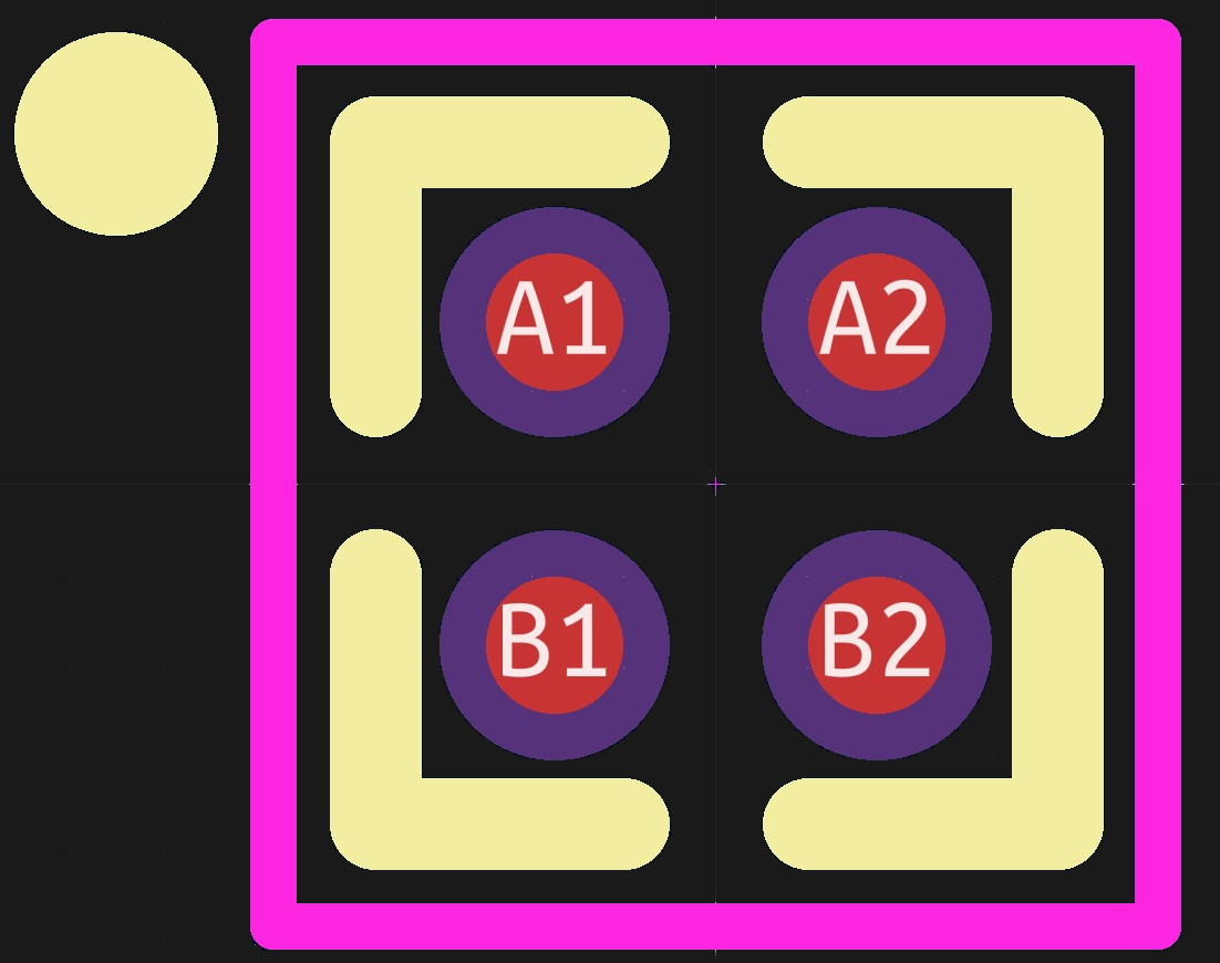
Second, force solder-mask-defined pads on every fine-pitch part where the copper gap is under 100 µm. That lets the mask overlap the pad edge and still leave a dam to the adjacent trace. The trade-off is a slightly smaller solderable area, but the isolation is more reliable than a collapsed dam.
Third, never let a high-speed or high-current trace run parallel to a pad at minimum spacing for more than a few hundred microns. The etch rate difference and the solder-mask registration both work against you. Route the escape, then pull the trace away.
Fourth, run a mask-dam DRC after the expansion rule is applied. Looking only at copper clearances is not enough. The mask layer is where the real manufacturing limit lives.
Finally, document the region-specific rules in the fab notes. "Minimum copper spacing 50 µm inside BGA keep-out, 100 µm elsewhere; solder mask dam minimum 75 µm after expansion" saves the CAM engineer from guessing and prevents the usual "can we open the spacing?" email three days before the panel is scheduled.
What Experience Actually Teaches
HDI pad to trace spacing is not a single number. It is the sum of etch undercut, mask registration, and the local density of the design. Push it everywhere and yield suffers. Push it only where the fan-out forces it, and keep the rest of the board at a comfortable process window, and the boards come back clean.
The designers who get this right treat the outer-layer clearance as a regional rule set rather than a global constraint. That single habit removes most of the manufacturing problems I still see on HDI reviews.