










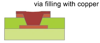
From a fabrication standpoint, the choice between copper-filled and resin-filled vias in HDI boards is driven by thermal demand, via-in-pad requirements, and cost tolerance more than by absolute reliability claims. Copper-filled vias deliver superior thermal and electrical conductivity and a flatter surface for via-in-pad soldering. Resin-filled vias (typically non-conductive epoxy followed by copper capping) are simpler, lower cost, and sufficient for many stacked-via and plugging applications where heat transfer is not critical.
Most shops default to resin fill with copper cap unless the design specifically needs the thermal path or the highest surface planarity that only solid copper fill can provide. Over-specifying copper fill adds process steps, plating time, and cost without benefit in many cases.
Where Copper Fill and Resin Fill Separate in Production
| Factor | Copper-Filled Vias | Resin-Filled Vias |
|---|---|---|
| Thermal conductivity | High – continuous copper path | Low – resin is a thermal barrier |
| Electrical conductivity | Excellent through the via | Limited to the plated barrel and cap |
| Via-in-pad suitability | Excellent – solid, planar surface | Good with proper capping and planarization |
| Surface flatness | Very high after planarization | Good after cap plating and planarization |
| Process complexity | Higher – specialized plating and planarization | Lower – fill, cure, then standard plating |
| Cost impact | Higher | Lower |
| Reliability under thermal cycling | Strong when process is controlled | Good; resin CTE can be a concern if not matched |
| Typical use cases | High-power, thermal vias, demanding via-in-pad | Standard HDI stacking, non-thermal via-in-pad |
Decision Matrix for HDI Via Fill Selection
| If your priority is… | Better Choice | Why |
|---|---|---|
| Maximum thermal transfer | Copper-filled | Continuous copper provides the best heat path |
| Lowest cost and simpler process | Resin-filled | Fewer specialized plating steps and lower material cost |
| Via-in-pad with high planarity | Copper-filled | Solid fill planarizes more consistently for fine-pitch soldering |
| Standard stacked microvias without heavy thermal load | Resin-filled | Adequate reliability at lower cost |
| High-reliability thermal cycling with heat dissipation | Copper-filled | Avoids resin CTE mismatch in the thermal path |
| High-volume consumer HDI | Resin-filled | Cost and throughput advantages dominate |
Thermal Performance Differences That Matter
Copper-filled vias create a continuous metallic thermal path from one side of the board to the other or between layers. This is the preferred solution when vias are used as thermal vias under power devices or when heat must be moved efficiently to an internal plane or heat sink. Resin-filled vias interrupt that path; the resin itself has very low thermal conductivity, so heat transfer relies mainly on the thin plated copper barrel and any copper cap.
In thermal simulations and real production, copper fill can reduce via thermal resistance by a factor of several times compared with resin fill. Designs that treat every via as a potential heat path should specify copper fill. Designs that only need mechanical plugging or stacked via support can stay with resin.
Via-in-Pad and Surface Planarity Considerations
Both fill methods can support via-in-pad when properly planarized, but copper fill generally produces a more consistent and flatter surface. After plating and planarization, the solid copper column resists dimpling better than a resin plug under the copper cap. Resin-filled vias can still achieve acceptable planarity for most fine-pitch BGAs, provided the fill process is void-free and the subsequent copper capping and planarization steps are tightly controlled.
From a fabrication standpoint, copper fill reduces the risk of solder voids or uneven paste volume on via-in-pad pads. Resin fill is acceptable for many consumer and mid-range applications but requires more process attention to avoid residual resin on the surface or incomplete filling that later causes plating defects.
Reliability Under Thermal and Mechanical Stress
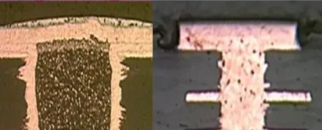
Copper-filled vias perform well in thermal cycling when the plating process is free of voids and the copper is properly annealed. The continuous copper matches the CTE of the surrounding copper features more closely than resin. Resin-filled vias introduce a polymer with higher CTE; under repeated thermal stress the resin can expand and contract differently from the copper barrel, potentially leading to cracks at the resin-copper interface or in the plated cap over long life.
In practice, well-controlled resin fill with appropriate CTE-matched epoxy and proper copper capping meets most reliability requirements for consumer and industrial HDI. Copper fill is preferred for high-reliability, high-power, or extreme temperature-cycling applications where the thermal path itself must remain intact.
Cost and Process Complexity Trade-offs
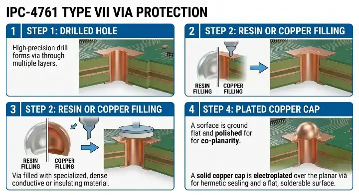
Copper filling requires specialized plating chemistry, longer plating times, and often multiple planarization steps to achieve a flat surface. These steps add direct cost and reduce throughput. Resin filling is typically a screen or vacuum fill process followed by curing, surface cleaning, and standard copper capping. The equipment and cycle time are lower, so unit cost is lower.
At volume, the cost difference can be significant, especially on boards with high via counts. Most fabricators will recommend resin fill with copper cap unless the thermal or planarity requirements clearly justify copper fill. Specifying copper fill "just in case" is one of the more common cost drivers we see in HDI designs that do not actually need the thermal performance.
Application Guidelines from the Shop Floor
Copper-filled vias are commonly specified under power ICs, RF amplifiers, LED arrays, and any location where heat must be moved efficiently through the board. They are also preferred for the most demanding via-in-pad fine-pitch applications where surface flatness directly affects solder joint quality. Resin-filled vias dominate in stacked microvia structures for signal routing, standard HDI smartphones and modules, and any design where the primary goal is to plug the via and provide a solderable surface without heavy thermal loading.
Hybrid approaches are common: copper fill only on thermal or critical via-in-pad locations, resin fill on the remaining vias. This balances performance and cost effectively.
How PCB Manufacturers Evaluate the Fill Decision
During DFM review we look first at whether the vias are thermal, signal, or via-in-pad, and at the expected power dissipation. If thermal conductivity is required or the via-in-pad pitch is extremely fine, copper fill is recommended. For standard stacked microvias used only for routing, resin fill with copper cap is the default. We also check the fabricator's process capability for void-free copper fill and for consistent resin fill and planarization.
Process risk is higher with copper fill because plating voids or incomplete fill can create reliability issues that are harder to detect. Resin fill risks include incomplete filling, resin residue on the surface, and CTE-related cracking if the wrong epoxy is used. Both processes require good planarization to keep the outer surface flat for subsequent imaging and soldering.
Most shops will push back on blanket copper-fill requirements when only a subset of vias actually need the thermal performance. Selective copper fill, where possible, improves both cost and yield.
Which Via Fill Should You Use?
Choose copper-filled vias if you:
- Need efficient heat transfer through the via (thermal vias)
- Require the highest surface planarity for fine-pitch via-in-pad
- Are designing high-power, high-reliability, or extreme thermal-cycling products
- Can accept the higher process cost and longer plating time
- Want continuous copper for both thermal and electrical performance
Choose resin-filled vias if you:
- Primarily need to plug vias for stacking or to create a solderable surface
- Do not require significant thermal conductivity through the via
- Are optimizing for cost and throughput in high-volume HDI
- Can achieve acceptable planarity with copper capping and planarization
- Are working with standard signal microvias rather than power or thermal paths
In many HDI designs the best approach is selective: copper fill only where thermal or critical via-in-pad performance is required, and resin fill elsewhere. This keeps cost under control while still delivering the necessary performance. Always match the fill method to the actual function of the via rather than applying one method across the entire board.
FAQ
Q1: Is copper-filled always more reliable than resin-filled?
A1: Not automatically. Copper fill is superior for thermal paths and can offer better long-term stability under heavy thermal cycling. Well-executed resin fill with proper CTE matching and copper capping meets reliability requirements for the majority of HDI applications. Process control matters more than the fill material alone.
Q2: Can resin-filled vias be used for via-in-pad?
A2: Yes. After resin fill, copper capping, and planarization, resin-filled vias support via-in-pad soldering for most fine-pitch packages. Copper fill generally provides slightly better and more consistent planarity, which becomes important at the tightest pitches or highest reliability levels.
Q3: How much more does copper fill cost compared with resin fill?
A3: The premium varies with via count and board size, but copper fill commonly adds noticeable cost because of longer plating times and specialized process steps. On high-via-count HDI boards the difference can be significant enough to justify selective copper fill only on critical vias.
Q4: Does copper fill eliminate the need for thermal vias elsewhere?
A4: Copper-filled vias can serve as effective thermal vias, but overall thermal design still depends on copper plane coverage, board thickness, and system-level heat sinking. Filling alone does not replace proper thermal layout.
Q5: What is the most common process risk with each method?
A5: For copper fill the main risks are plating voids and incomplete fill. For resin fill the risks are incomplete filling, surface resin residue, and potential CTE mismatch cracking over life. Both require effective planarization to keep the outer surface flat.
Q6: Can I mix copper-filled and resin-filled vias on the same board?
A6: Yes, and this is often the most cost-effective approach. Use copper fill only on thermal or critical via-in-pad locations and resin fill on the remaining signal or stacking vias. Confirm with the fabricator that selective processing is supported.






