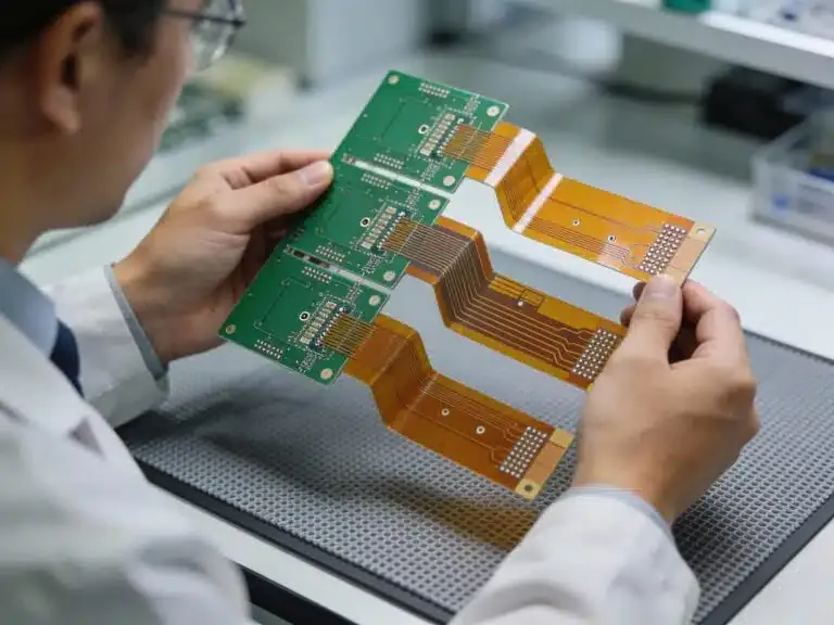
Introduction
The advent of 5G technology marks a transformative era for consumer electronics and IoT devices. This next-generation connectivity promises unprecedented speed, low latency, and massive device integration. However, achieving these benefits hinges on meticulous PCB design. Printed Circuit Boards are the backbone of electronic systems, and with 5G, the demands for signal integrity, thermal management, and compact layouts intensify. Engineers face unique challenges in ensuring that 5G PCB designs support high-frequency signals without interference or loss. For electrical engineers, understanding the interplay between design principles and 5G requirements is critical. This article explores how optimized PCB design unlocks the full potential of 5G, focusing on key aspects like signal integrity and best practices tailored for IoT devices and consumer electronics.
What Is 5G PCB Design and Why It Matters
5G PCB design refers to the specialized process of creating circuit boards that support the high-frequency, high-speed requirements of 5G technology. Unlike previous generations, 5G operates at millimeter-wave frequencies, often exceeding 24 GHz, alongside sub-6 GHz bands. This shift demands exceptional signal integrity and precise impedance control to prevent data loss or interference. For consumer electronics like smartphones and wearables, as well as IoT devices such as smart sensors, the PCB must handle dense component layouts while maintaining performance.
The importance of 5G PCB design lies in its direct impact on connectivity and reliability. Poorly designed boards can lead to signal degradation, increased latency, or electromagnetic interference, undermining the advantages of 5G. Electrical engineers must prioritize material selection, layer stacking, and routing strategies to meet these stringent needs. As 5G adoption grows across industries, mastering PCB design becomes a cornerstone for innovation and functionality in modern electronics.
Technical Principles of 5G PCB Design
High-Frequency Signal Challenges
5G technology introduces signals at much higher frequencies than 4G, often in the range of millimeter waves. These signals are prone to attenuation over short distances and are sensitive to obstacles. On a PCB, this translates to potential signal loss through dielectric materials and conductor paths. Maintaining signal integrity requires minimizing parasitic capacitance and inductance, which can distort high-speed data transmission. Engineers must account for skin effect, where current flows near the conductor surface at high frequencies, increasing resistance.
Material Selection for 5G
The choice of substrate material is pivotal in 5G PCB design. Standard FR-4 materials, while cost-effective, often fail to meet the low dielectric constant and loss tangent needed for high-frequency applications. Low-loss laminates with stable dielectric properties are preferred to reduce signal attenuation. These materials help maintain consistent impedance across the board, a critical factor for signal integrity in consumer electronics and IoT devices.
Impedance Control and Routing
Impedance mismatches can cause signal reflections, leading to data errors. For 5G PCB designs, controlled impedance traces are essential, especially for differential pairs used in high-speed communication. Routing must avoid sharp bends and maintain uniform trace widths to prevent disruptions. Additionally, vias should be minimized or optimized as they introduce inductance at high frequencies. Proper grounding techniques, including ground planes, further enhance signal integrity by reducing noise.
Thermal Management in High-Density Designs
5G devices often pack powerful processors and transceivers into compact spaces, generating significant heat. Poor thermal management can degrade component performance and affect signal integrity. PCB design must incorporate thermal vias, heat sinks, or copper pours to dissipate heat effectively. This is especially crucial for IoT devices, where space constraints limit cooling options. Engineers must balance thermal needs with electrical performance to ensure reliability.
Related Reading: What is The Layer Stackup Design for optimum 5G Performance
Best Practices for 5G PCB Design
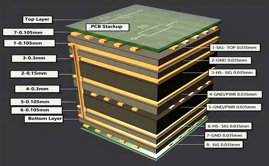
Multilayer Board Configurations
Using multilayer boards is a common strategy in 5G PCB design to accommodate complex routing and grounding needs. A typical stack-up might include dedicated ground and power planes to isolate high-speed signals from noise sources. For instance, a six-layer board could allocate top and bottom layers for signals, with internal layers for ground and power distribution. This configuration minimizes crosstalk and enhances signal integrity, a priority for consumer electronics operating on 5G networks.
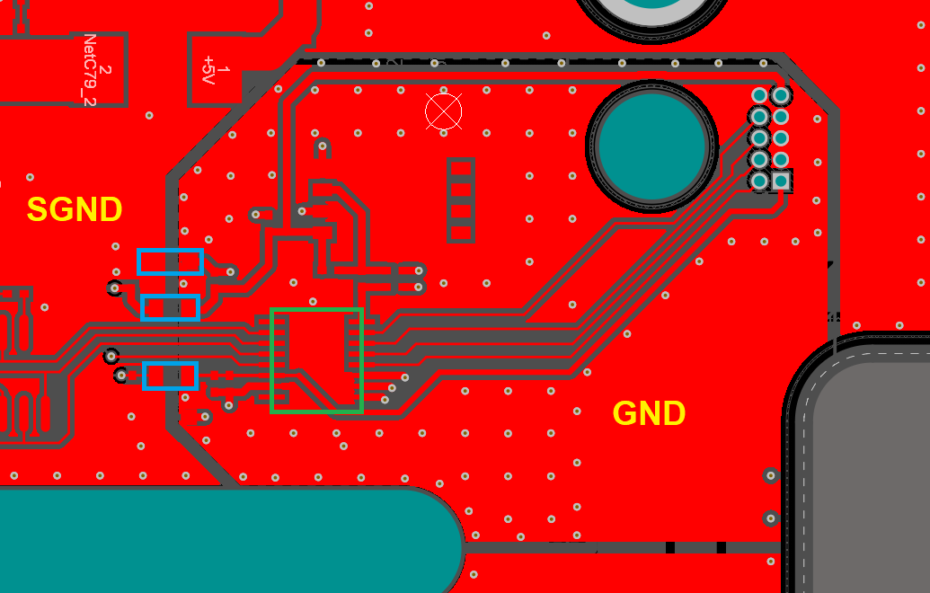
Grounding and Shielding Techniques
Effective grounding is non-negotiable in 5G PCB design. Continuous ground planes reduce electromagnetic interference and provide a stable reference for signals. Engineers should place ground vias strategically near high-speed components to create low-impedance return paths. Shielding, such as using guard traces or metal enclosures, further protects sensitive signals from external noise, a critical consideration for IoT devices in dense environments.
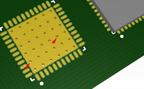
Component Placement and Density
Component placement directly influences signal performance in 5G designs. High-frequency components, like RF transceivers, should be placed close to their matching networks to minimize trace lengths. Decoupling capacitors must be near power pins to filter noise effectively. For densely packed consumer electronics, engineers must optimize layouts to avoid interference between analog and digital sections, ensuring robust operation under 5G conditions.
Adherence to Industry Standards
Following established guidelines ensures consistency and reliability in 5G PCB design. Standards like IPC-6012E provide specifications for rigid board performance, while IPC-A-600K outlines acceptability criteria for printed boards. Compliance with these standards helps engineers validate signal integrity and manufacturing quality, reducing risks in high-stakes applications like IoT devices and consumer electronics.
Simulation and Prototyping
Before finalizing a design, simulation tools are invaluable for predicting performance. These tools analyze signal integrity, thermal behavior, and electromagnetic compatibility under 5G conditions. Prototyping and iterative testing further validate the design, allowing engineers to identify issues like crosstalk or impedance mismatches. This step is essential for complex boards destined for consumer electronics, where reliability is paramount.
Related Reading: How to Design 5G PCB Layout Guidelines?
Insight: Balancing Cost and Performance in 5G PCB Design
For electrical engineers, one persistent challenge in 5G PCB design is balancing cost with performance. High-performance materials and intricate multilayer configurations often increase production expenses. However, cutting corners on material quality or layer count can compromise signal integrity, leading to costly redesigns or field failures. A practical approach involves prioritizing critical areas, such as RF signal paths, for premium materials while using standard substrates elsewhere. Additionally, optimizing trace layouts to reduce via count can lower manufacturing complexity without sacrificing performance. Collaboration between design and manufacturing teams early in the process ensures that cost-effective solutions align with 5G requirements. This balance is especially vital for mass-produced consumer electronics and scalable IoT devices, where margins are tight, and reliability is non-negotiable.
Conclusion
Unlocking the power of 5G through PCB design demands a deep understanding of high-frequency challenges and innovative solutions. From selecting low-loss materials to implementing robust grounding techniques, every aspect of design influences signal integrity and overall performance. For consumer electronics and IoT devices, optimized 5G PCB design ensures seamless connectivity, reduced latency, and reliable operation in demanding environments. Electrical engineers must adhere to industry standards and leverage simulation tools to refine their designs. By embracing best practices and balancing cost with performance, the full potential of 5G can be realized, paving the way for groundbreaking advancements in technology and communication.
FAQs
Q1: How does 5G PCB design differ from 4G for consumer electronics?
A1: 5G PCB design focuses on supporting higher frequencies, often above 24 GHz, compared to 4G's lower bands. This requires materials with low dielectric loss and precise impedance control to maintain signal integrity. Additionally, 5G designs often need denser layouts and advanced thermal management for compact consumer electronics, ensuring performance without overheating or interference in high-speed applications.
Q2: What role does signal integrity play in 5G PCB for IoT devices?
A2: Signal integrity is crucial in 5G PCB design for IoT devices as it ensures data transmission without loss or noise. High-frequency 5G signals are prone to attenuation and interference, which can disrupt connectivity in sensors or smart devices. Proper routing, grounding, and material selection minimize these issues, enabling reliable operation in diverse, often crowded, IoT environments.
Q3: Why is material selection critical in 5G PCB design?
A3: Material selection in 5G PCB design directly impacts signal performance at high frequencies. Low-loss dielectrics reduce attenuation and maintain impedance stability, vital for 5G applications. Poor materials can cause signal degradation, affecting speed and reliability in consumer electronics. Choosing the right substrate ensures consistent performance, especially under the demanding conditions of 5G networks.
Q4: What standards should guide 5G PCB design for signal integrity?
A4: Standards like IPC-6012E and IPC-A-600K are essential for 5G PCB design. IPC-6012E outlines performance specifications for rigid boards, while IPC-A-600K defines acceptability criteria, ensuring quality. Adhering to these guidelines helps maintain signal integrity by standardizing manufacturing and design processes, critical for high-frequency 5G applications in various devices.
References
IPC-6012E — Qualification and Performance Specification for Rigid Printed Boards. IPC, 2020.
IPC-A-600K — Acceptability of Printed Boards. IPC, 2020.