Understanding Soldering Defects in PCB Assembly
Soldering is a critical process in printed circuit board (PCB) assembly, directly influencing the reliability and performance of electronic devices. Even minor soldering defects can lead to significant issues, including intermittent connections, signal degradation, or complete failure of the assembly. For electrical engineers, understanding common soldering defects such as cold solder joints, solder bridges, insufficient solder, and solder voids is essential to ensure robust designs and high-quality manufacturing outcomes. These defects not only compromise the functionality of a PCB but also increase repair costs and reduce product lifespan. This article explores the nature of these soldering issues, their root causes, and their impact on PCB reliability. By addressing these challenges with industry-standard practices, engineers can enhance the durability and performance of electronic systems.
What Are Soldering Defects and Why Do They Matter in PCBA
Soldering defects refer to imperfections in the solder joint formation during PCBA assembly, resulting in unreliable electrical or mechanical connections. These defects are a primary concern because they undermine the integrity of the connection between components and the PCB, leading to potential failures in the field. For electrical engineers, soldering defects are critical as they affect signal integrity, power delivery, and overall system stability. Poor solder joints can cause increased resistance, overheating, or open circuits, impacting the performance of high-speed or high-power applications. Adhering to recognized standards like IPC J-STD-001H, which outlines requirements for soldered electrical and electronic assemblies, helps in identifying and mitigating these issues. Addressing soldering defects early in the design or manufacturing phase is vital to achieving long-term reliability and meeting stringent quality expectations in industries such as aerospace, automotive, and medical electronics.
Root Causes of Common Soldering Defects in PCB Assembly
Understanding the root causes of soldering defects is the first step toward prevention. Several factors during the assembly process contribute to issues like cold solder joints, solder bridges, insufficient solder, and solder voids. These causes often relate to process parameters, material properties, or equipment setup.
- Temperature Control Issues: Inadequate heating or cooling during soldering can prevent proper wetting of the solder, leading to cold solder joints. If the soldering iron or reflow oven does not reach the required temperature, the solder may not fully melt or bond with the component leads and pads.
- Contamination: Flux residues, oxides on component leads, or dirty PCB surfaces can interfere with solder adhesion. This often results in insufficient solder or weak joints that fail under stress.
- Improper Solder Paste Application: Uneven or inadequate solder paste deposition during surface mount technology (SMT) processes can cause solder voids or insufficient solder, compromising joint strength.
- Component Misalignment: Misaligned components during placement can lead to solder bridges, where excess solder connects adjacent pads or leads, causing short circuits.
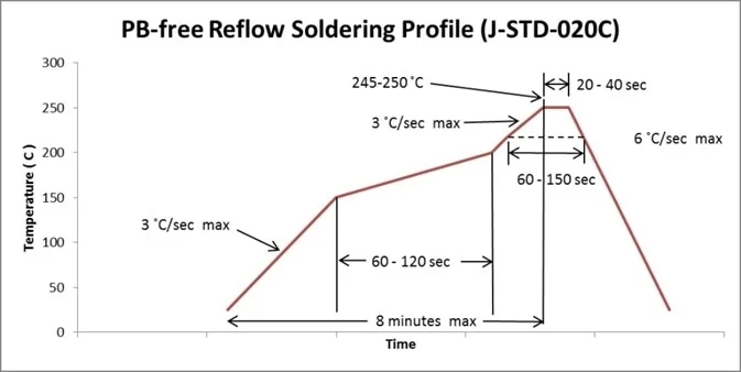
- Reflow Profile Errors: An incorrect reflow profile, such as rapid cooling or insufficient soak time, can trap gases within the solder joint, forming voids that weaken the connection.
Standards like IPC-A-610H, which defines acceptability criteria for electronic assemblies, provide guidelines for identifying and controlling these causes. By adhering to such standards, engineers can minimize the occurrence of soldering defects during production.
Common Soldering Defects on PCB: Types, Causes & Reliability Impact
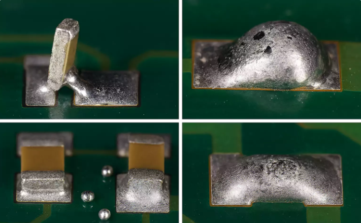
Cold Solder Joints
Cold solder joints occur when the solder does not fully melt or wet the surfaces of the component lead and PCB pad, resulting in a dull, grainy appearance. This defect often stems from insufficient heat or rapid cooling during the soldering process. The impact on PCB reliability is significant, as cold solder joints create high-resistance connections that can lead to intermittent failures or complete open circuits. Over time, thermal cycling or mechanical stress can cause these joints to crack, further degrading performance. Electrical engineers must ensure proper soldering temperatures and durations as outlined in IPC J-STD-001H to prevent this issue.
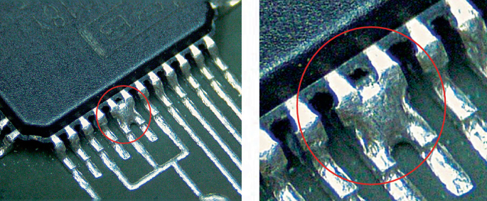
Solder Bridges
Solder bridges form when excess solder creates an unintended connection between adjacent pads or leads, often due to improper paste application or component misalignment. This defect causes short circuits, disrupting the intended electrical pathways and potentially damaging components. The reliability of the PCB is compromised, especially in high-density designs where spacing is minimal. Following guidelines from IPC-A-610H for acceptable solder joint formation can help in detecting and preventing solder bridges during inspection.
Insufficient Solder
Insufficient solder occurs when there is not enough solder material to form a proper joint between the component and the pad. This can result from inadequate solder paste deposition or poor wetting due to contamination. The impact includes weak mechanical connections that may fail under vibration or thermal stress, leading to open circuits. For critical applications, this defect reduces PCB reliability and necessitates rework. Adhering to process controls specified in IPC J-STD-001H ensures adequate solder volume for robust joints.
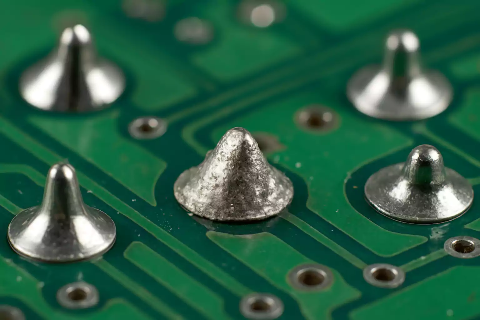
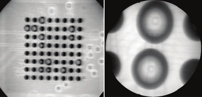
Solder Voids
Solder voids are gas pockets trapped within the solder joint, often caused by outgassing during the reflow process or improper flux activity. These voids reduce the effective contact area, increasing electrical resistance and thermal impedance. In high-power applications, this can lead to overheating and joint failure, significantly impacting PCB reliability. Standards such as IPC-A-600K, which addresses acceptability of printed boards, provide criteria for evaluating void levels in solder joints to maintain quality.
Suggested Reading: Common SMT PCB Assembly Defects
Best Practices to Prevent Soldering Defects in PCB Manufacturing
Preventing soldering defects requires a combination of process optimization, quality control, and adherence to industry standards. Electrical engineers can implement the following best practices to enhance PCB reliability.
- Optimize Reflow Profiles: Ensure the reflow oven temperature profile matches the solder paste specifications. A well-defined preheat, soak, and reflow phase minimizes the risk of cold solder joints and solder voids. Guidelines from IPC J-STD-001H provide detailed recommendations for thermal profiles.
- Use Clean Materials: Maintain cleanliness of PCB surfaces, component leads, and soldering equipment. Proper flux application removes oxides and contaminants, reducing the likelihood of insufficient solder or weak joints.
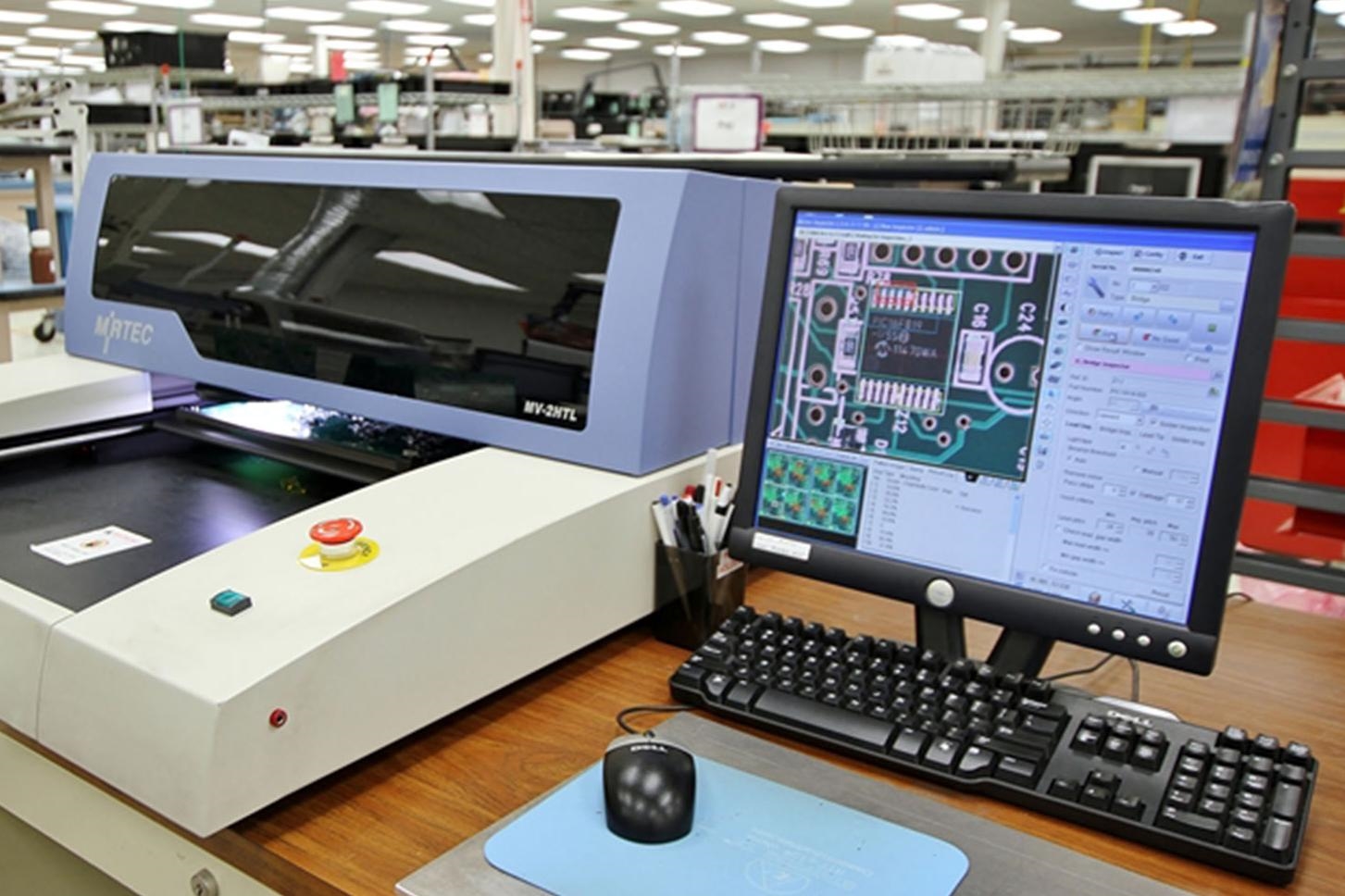
- Implement Automated Inspection: Utilize automated optical inspection (AOI) and X-ray inspection to detect solder bridges and voids early in the assembly process. These methods align with acceptability criteria in IPC-A-610H, ensuring defective joints are identified before final testing.
- Control Solder Paste Application: Employ precise stencil printing techniques to deposit the correct amount of solder paste. This prevents insufficient solder and reduces the risk of solder bridges in high-density areas.
- Train Personnel: Ensure assembly technicians are trained in manual soldering techniques and understand the importance of heat control and joint formation. Certification programs based on IPC J-STD-001H can standardize skills across teams.
Troubleshooting & Rework for PCB Soldering Defects
When soldering defects are detected, troubleshooting becomes a critical task for electrical engineers. A systematic approach can help identify and resolve issues without compromising the PCB. For cold solder joints, reheating the joint with a soldering iron to achieve proper wetting is often effective, provided the thermal limits of components are respected. Solder bridges can be corrected by removing excess solder with a desoldering wick or suction tool, ensuring no damage to adjacent pads. Insufficient solder may require adding more solder material, while maintaining control to avoid bridges. For solder voids, especially in ball grid array (BGA) components, X-ray inspection per IPC-A-600K standards can quantify void levels and determine if rework is necessary. Documenting defect patterns and correlating them with process parameters helps in preventing recurrence during future production runs.
Suggested Reading: Prevent SMT Soldering Defects: Tips
Conclusion
Soldering defects such as cold solder joints, solder bridges, insufficient solder, and solder voids pose significant challenges to PCB reliability. These issues, if unaddressed, can lead to electrical failures, mechanical weaknesses, and reduced product lifespan. By understanding the causes and implementing practical solutions aligned with industry standards like IPC J-STD-001H and IPC-A-610H, electrical engineers can mitigate these defects effectively. A focus on process control, material quality, and inspection techniques ensures robust solder joints that withstand the demands of modern electronic applications. Prioritizing these practices not only enhances PCB performance but also builds trust in the quality and durability of the final product.
FAQs
Q1: What are the main causes of cold solder joints on a PCB?
A1: Cold solder joints often result from insufficient heat during soldering, preventing proper wetting of the component lead and pad. Other causes include rapid cooling or contamination on surfaces. These defects create high-resistance connections, leading to unreliable performance. Following thermal guidelines in industry standards helps ensure adequate heat application and joint integrity during assembly.
Q2: How do solder bridges affect PCB reliability in high-density designs?
A2: Solder bridges cause short circuits by connecting adjacent pads or leads, disrupting electrical pathways. In high-density designs, where spacing is tight, this defect severely impacts PCB reliability. It can damage components or cause system failures. Automated inspection and precise solder paste application are essential to prevent bridges and maintain circuit integrity.
Q3: Why is insufficient solder a concern for PCB durability?
A3: Insufficient solder leads to weak mechanical and electrical connections between components and pads. This defect increases the risk of open circuits under vibration or thermal stress, reducing PCB durability. It often stems from poor paste deposition or contamination. Ensuring proper solder volume per industry criteria is critical for long-term reliability.
Q4: How can solder voids be detected and minimized in PCB assembly?
A4: Solder voids are detected using X-ray inspection, which reveals gas pockets within joints. These voids increase resistance and thermal impedance, affecting reliability. Minimizing them involves optimizing reflow profiles and using appropriate flux to reduce outgassing. Adhering to acceptability standards ensures void levels remain within safe limits for performance.
References
IPC J-STD-001H — Requirements for Soldered Electrical and Electronic Assemblies. IPC, 2021.
IPC-A-610H — Acceptability of Electronic Assemblies. IPC, 2021.
IPC-A-600K — Acceptability of Printed Boards. IPC, 2020.


