Selecting Test Probes for SMT PCBs: A Comprehensive Guide
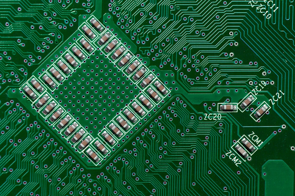
Discover how to choose the right SMT test probes for accurate functional testing of PCBs, covering factors like test point size, fine pitch requirements, resistance, and maintenance.
Discover how to choose the right SMT test probes for accurate functional testing of PCBs, covering factors like test point size, fine pitch requirements, resistance, and maintenance.
Explore the essential design considerations for high Tg PCBs including stackup planning impedance control via design and thermal expansion management to ensure reliable performance in high temperature automotive and aerospace applications.
Optimize High Tg PCB manufacturing. This guide details lamination, reflow, and wave soldering processes to ensure reliability for automotive and aerospace electronics.
Explore sustainable electronics with Polylactic Acid (PLA) as a PCB substrate. This guide covers PLA's benefits, challenges, and applications in biodegradable flexible PCBs.
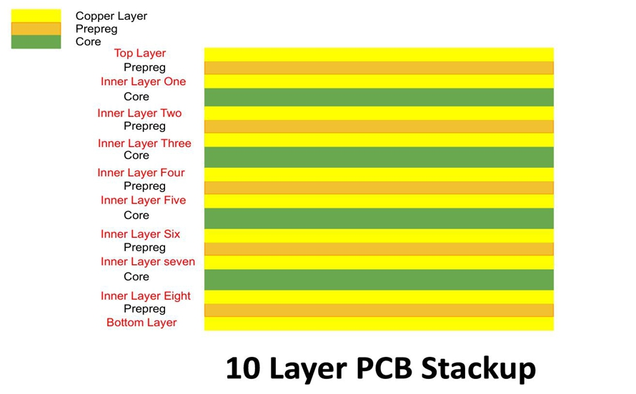
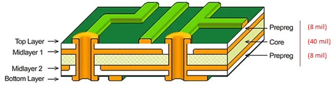
Discover how a 10-layer PCB stackup optimizes high-speed designs. Learn about impedance control, signal integrity, and material selection for peak performance in complex circuits.
Explore FR-4 PCB design for wearable technology: Master miniaturization, low-power layouts, flexible FR-4, sensor integration, Bluetooth optimization, and fitness tracker specifics. Achieve lightweight boards under 5g with IPC-4101C standards—key for 2025 smartwatches.
Enhance high temperature PCB reliability with High Tg PCBs. Learn thermal management for automotive and aerospace electronics.
Dive into multilayer FR-4 PCBs: Explore stackup strategies, PCB routing techniques, via design, signal integrity, power distribution, and high-density manufacturing. Boost performance with IPC-4101C standards—essential for 2025 IoT and 5G innovations.
Discover PCB surface finish types like HASL, ENIG, immersion silver, OSP, and ENEPIG: Optimize for solderability, corrosion protection, and reliability on FR-4 boards. Achieve 99% yields with IPC-4552 standards—essential for 2025 high-density assembly.
A comprehensive guide to 12-layer PCB stackup design, focusing on impedance control, signal integrity, material selection, design rules, and cost optimization for high-speed electronics.
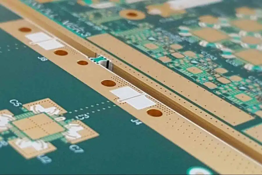
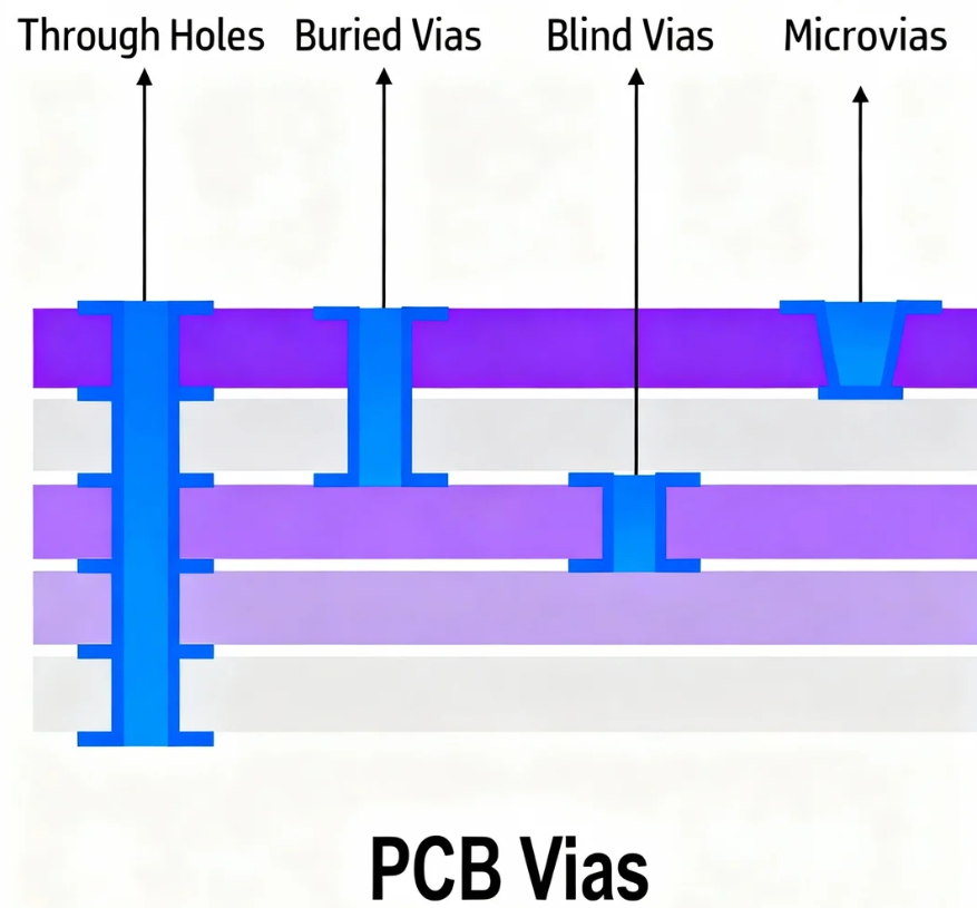
Explore stacked vias in High-Density Interconnect (HDI) PCBs, covering their design principles, manufacturing processes, key reliability considerations, and cost implications.
Learn how to design an efficient 4-layer PCB stackup to improve signal integrity, minimize noise, and optimize performance for modern electronic devices.