Overview
Solar cell conversion efficiency is limited by optical absorption, carrier transport, and carrier collection. For single-crystal silicon solar cells, because photons with energy above the bandgap lose excess energy before being converted, the theoretical maximum conversion efficiency is about 28%. In practice, additional losses make actual efficiencies much lower. Improving efficiency therefore requires identifying and minimizing these losses.
Efficiency loss mechanisms
Improving solar cell efficiency is a primary goal in the solar photovoltaics industry. In general, a 1% absolute gain in solar cell efficiency can reduce system cost significantly.
Studies indicate that the main factors limiting crystalline silicon solar cell conversion efficiency fall into two categories:
- Optical losses, including front-surface reflection, shading by front metallization fingers, and lack of absorption in the long-wavelength region.
- Electrical losses, including recombination of photogenerated carriers at surfaces and in the bulk, contact resistance between semiconductor and metal fingers, and metal-semiconductor contact resistance.
The most critical issue is reducing recombination of photogenerated carriers, which directly affects open-circuit voltage. Front-surface heavy-doped diffusion layers introduce many recombination centers. When minority-carrier diffusion length is comparable to or exceeds wafer thickness, back-surface recombination also strongly influences cell performance.
Methods to improve conversion efficiency
Common approaches to improve crystalline silicon solar cell efficiency include:
1. Light-trapping structures
High-efficiency single-crystal silicon cells typically use chemical etching to form a textured surface; the textured surface can reduce reflectance to below 10%. A more advanced method is reactive ion etching (RIE), which is orientation-independent and suitable for thinner wafers. RIE typically uses SF6/O2 gas: F radicals chemically etch silicon to form volatile SiF4, while O radicals form SixOyFz that passivates sidewalls, producing a textured surface. Commercial equipment can produce textured reflectance in the low single digits.
2. Anti-reflection coatings
Anti-reflection coatings (ARCs) are dielectric films with optimized refractive index and thickness that cause reflected waves to destructively interfere, minimizing front-surface reflectance. Single-crystal silicon cells commonly use single- or double-layer ARCs such as TiO2, SiO2, SnO2, ZnS, or MgF2. Applying an ARC to a textured surface can reduce reflectance to around 2%.
3. Surface passivation
Passivation reduces carrier recombination at specific regions. Effective passivation methods include thermal oxide passivation, atomic hydrogen passivation, and surface diffusion of phosphorus, boron, or aluminum. Thermal oxide forms a silicon dioxide layer on both front and back surfaces to suppress surface recombination. Atomic hydrogen passivates dangling bonds at the silicon surface, reducing recombination centers.
4. Back-surface field (BSF)
In p-type cells, a heavily doped P+ layer at the rear forms a P+/P structure that creates a built-in field toward the P+ side. This field separates and accumulates photogenerated carriers, adding a photovoltage with polarity that improves the cell open-circuit voltage (Voc). The back field also accelerates carriers, effectively increasing their collection length and improving short-circuit current density (Jsc).
5. Improved substrate material
Using high-quality silicon, such as n-type silicon, provides longer carrier lifetimes, reduced boron-oxygen degradation after junction formation, better conductivity, and lower saturation current.
Notable high-efficiency crystalline silicon cell architectures
PERL (Passivated Emitter and Rear Locally-diffused) cells
PERL cells combine a passivated emitter with locally diffused boron regions on the rear for localized contacts. In 1990, J. Zhao at the University of New South Wales implemented local boron diffusion at rear contact openings, demonstrating PERL cells with efficiencies up to 24.7%, approaching theoretical limits.
Key features that enable PERL efficiency:
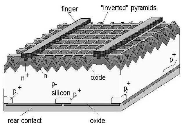
- “Inverted pyramid” front surface texturing, which offers lower reflectance than conventional texturing and improves Jsc.
- Phosphorus diffusion zoning: heavy phosphorus under contact fingers reduces contact resistance, while lighter phosphorus in illuminated regions minimizes lateral resistive losses and preserves short-wavelength response.
- Localized small-area boron diffusion on the rear forms P+ regions that reduce rear-contact resistance and provide a boron back-surface field; evaporated aluminum rear contacts serve as good back reflectors, further improving conversion efficiency.
- Double-sided passivation: emitter-side passivation reduces surface states and front-side recombination; rear passivation reduces reverse saturation current density and improves spectral response. However, PERL fabrication requires several photolithography steps, making it relatively complex and costly.
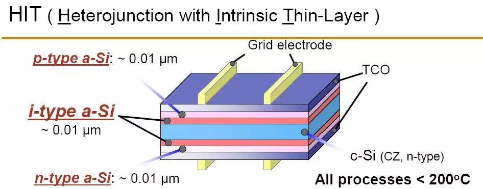
HIT (Heterojunction with Intrinsic Thin layer) cells
HIT cells use thin intrinsic a-Si:H layers to form heterojunctions with crystalline silicon. Typical fabrication: deposit a thin intrinsic a-Si:H layer and a p-type a-Si:H layer by PECVD on a textured n-type CZ-Si wafer front; deposit a thin intrinsic a-Si:H and n-type a-Si:H on the rear; sputter transparent conductive oxide (TCO) on both sides; then screen-print Ag electrodes on the TCO. All processing is performed below 200 °C, which helps preserve carrier lifetime and reduces energy consumption.
Reasons for high HIT efficiency:
- Low-temperature processing preserves bulk carrier lifetime.
- Double-sided junctions can utilize backside light.
- Amorphous silicon surface layers have strong optical absorption for specific wavelengths.
- Using n-type wafers provides longer carrier lifetimes and lower susceptibility to light-induced degradation compared with p-type wafers; thin wafers help carriers diffuse across the substrate to be collected by electrodes.
- Textured wafers reduce front-surface reflection.
- Hydrogen generated during PECVD passivates interface defects between amorphous and crystalline silicon, a major factor in achieving high efficiency.
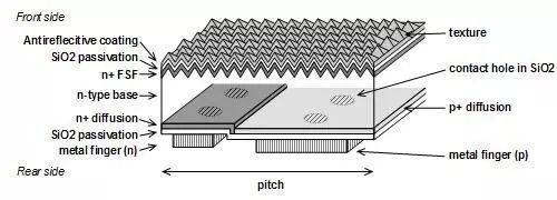
IBC (Interdigitated Back-contact) cells
IBC cells place all contacts on the rear surface: positive and negative electrodes are interdigitated on the back, leaving the front free of metal fingers. Advantages include reduced front-side shading, lower module assembly cost, and improved aesthetics.
Because carriers must traverse the full wafer thickness to reach back-surface junctions, IBC cells require wafers with high carrier lifetime, typically n-type FZ monocrystalline silicon. The front surface uses a silicon oxide or oxide/nitride stack combined with an N+ emitter and textured surface for antireflection. The rear forms alternating P+ and N+ diffusion regions with metal contact openings in the oxide to connect electrodes to emitter or base regions. The interdigitated rear contacts cover most of the rear surface, facilitating current extraction.
The rear-contact design achieves effectively zero front-side shading and increased light utilization, but fabrication is complex. Key process challenges include precise P+ diffusion, heavy diffusion under metal fingers, and laser-fired contacts.
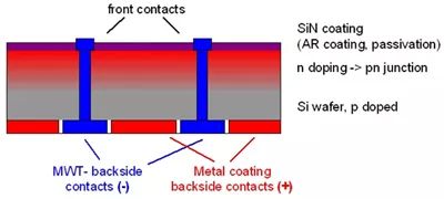
MWT (Metallization Wrap-Through) cells
MWT cells route front-side collected current to the rear through laser-drilled vias. This approach is commonly applied to p-type multicrystalline wafers. By transferring front-side current to the rear, MWT can increase per-cell output by about 2%, and module-level gains of about 9% have been reported when cells are interconnected.
MWT process challenges include alignment and reproducibility of laser drilling and trench isolation, control of via size and shape, laser- and substrate-induced damage, and metallization filling of vias. Typical MWT wafers require on the order of 200 through-vias per wafer.
EWT (Emitter Wrap-Through) cells
EWT cells also transfer grid lines to the rear, but unlike MWT, EWT transfers the emitter fingers themselves to the back. Power-transferring gridlines are routed through many small vias that connect front and rear. EWT typically requires far more vias per wafer than MWT—on the order of 20,000 per wafer—so high-speed laser drilling is a prerequisite for commercial production.
EWT eliminates front-side fingers and electrodes, simplifying module assembly and removing shading loss while enabling bifacial carrier collection and substantially increasing photocurrent. Industrial-scale EWT manufacturing uses screen printing and laser processing and places specific demands on wafer quality and process control, including damage-free laser cutting, metallization filling depth, and emitter series resistance optimization. Early EWT devices produced with this geometry have demonstrated efficiencies above 17%.
Laser-etched groove buried-contact cells
The laser-etched groove buried-contact technique developed at UNSW uses laser scribing to form grooves on the silicon surface that are subsequently filled with metal, creating localized buried contacts. After emitter diffusion, a laser is used to scribe grooves about 20 μm wide and 40 μm deep on the front. The grooves are cleaned, a heavy phosphorus diffusion is applied, and metal electrodes are plated into the grooves. Because the electrodes lie within the silicon, front-side shading is reduced and current density is increased, yielding efficiencies around 19.6% in experiments.
Compared with conventional front-side metallization, buried contacts reduce front-side shading, increase current density, improve collection of carriers from the base due to deeper electrode penetration, and lower finger-to-substrate contact resistance via heavy diffusion under the fingers, thereby raising Voc.
Buried-contact cells retain features of high-efficiency cells but avoid some complex high-cost processes, making them suitable for large-area, low-cost wafer production.
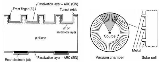
OECO (Obliquely Evaporated Contact) cells
OECO cells use oblique evaporation to form metal contacts on a structured surface and are based on a metal-insulator-semiconductor (MIS) contact scheme. This approach can be simpler and lower-cost than other high-efficiency architectures because it does not require photolithography, contact firing, heavy under-diffusion beneath electrodes, or high-temperature processes to form high-quality contacts. OECO electrodes are formed by obliquely evaporating low-cost aluminum onto the sidewalls of shallow surface grooves over a thin tunnel oxide. A PECVD nitride layer then provides passivation and antireflection.
OECO advantages include the ability to evaporate many contacts in one step, good contact quality on the thin tunnel oxide, and modest efficiency loss when scaling active area from 4 cm2 to 100 cm2 (reported drop from 21.1% to about 20%), indicating scalability for manufacturing.
OECO cells use an array of square grooves on the surface. A shallow n+ emitter sits on the top surface with a thin tunnel oxide above it. Aluminum is obliquely evaporated onto the groove sidewalls to form contacts; PECVD nitride is applied as passivation and ARC.
OECO characteristics:
- Electrodes on groove sidewalls help increase Jsc.
- MIS-based design can achieve high Voc and fill factor.
- High-quality evaporated metal contacts.
- Shallow emitters can be optimized without contact limitations.
- High-quality low-temperature surface passivation.
Outlook
With ongoing industrial development and the increasing importance of renewable energy, research teams worldwide continue to seek ways to raise efficiency and reduce cost. While new cell types are emerging, crystalline silicon solar cells are expected to remain dominant in the near term due to their favorable properties and relatively high conversion efficiencies.