Introduction
There are several established methods for handling supply-voltage reversal. The simplest is a diode between the supply and the load, but the diode's forward drop causes extra power loss. Although simple, a diode is unsuitable for portable or backup applications because the battery must both source current when not charging and sink current when charging. Another approach uses one of the MOSFET circuits shown in Figure 1.
Figure 1: traditional load-side reverse protection
Load-Side MOSFET Protection
This approach is superior to a diode for load-side circuits because the battery voltage enhances the MOSFET, producing lower drop and substantially higher conductance. The NMOS version is preferable to the PMOS version for discrete designs because NMOS transistors often have higher conductivity, lower cost, and better availability. In both versions the MOSFETs conduct when the battery voltage is positive and disconnect when the battery voltage is reversed. The MOSFET's physical drain becomes the power terminal, because it is at the higher potential in the PMOS case and at the lower potential in the NMOS case. Since MOSFETs are electrically symmetric in the triode region, they conduct well in both directions. With this method, devices must have VGS and VDS ratings higher than the maximum battery voltage.
Unfortunately, this method works only for load-side protection and cannot be used with a circuit capable of charging the battery. A battery charger can generate voltage that re-enables the MOSFET and reconnects to a reversed battery. Figure 2 shows an NMOS example with a faulty/reversed battery.
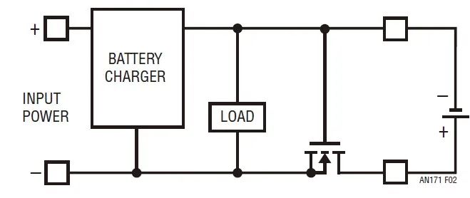
Figure 2: load-side protection with a battery charger
When the battery is connected, the charger is idle and the load and charger are safely decoupled from the reversed battery. But if the charger becomes active (for example, when an input power connector is attached), it can create a voltage between the NMOS gate and source that enhances the NMOS and allows current to flow. That situation is illustrated in Figure 3.
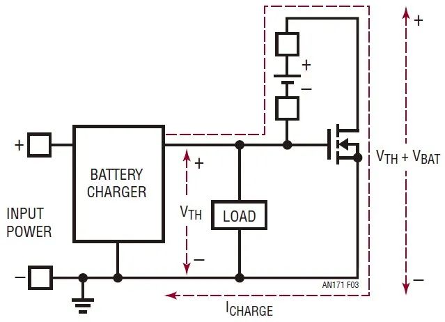
Figure 3: traditional reverse-battery protection fails with a battery charger present
Although the load and charger are isolated from the reversed battery, the protecting MOSFET can now dissipate excessive power. The charger effectively becomes a battery discharger. When the charger supplies enough gate drive to allow charge current through the MOSFET, an equilibrium is reached. For example, if a strong MOSFET has a threshold voltage VTH of roughly 2 V and the charger can provide current at 2 V, the charger output will settle near 2 V (the MOSFET drain sits at VBAT + 2 V). Dissipation in the MOSFET is I_CHARGE × (VTH + VBAT), which heats the MOSFET until heat is removed from the printed circuit board. The PMOS version shows the same behavior.
The following sections describe two alternative approaches, each with advantages and tradeoffs.
N-Channel MOSFET Design
The first approach uses an NMOS isolator, as shown in Figure 4.
The algorithm is: if the battery voltage exceeds the charger output voltage, the isolation MOSFET must be disabled.
As with the earlier NMOS method, MN1 is placed on the low-voltage side between the charger/load and the battery terminal. However, MP1 and Q1 now provide a detection circuit that disables MN1 in the event of a reversed battery. A reversed battery raises MP1's source above its gate, allowing current through MP1. MP1's drain then supplies current through R1 to Q1's base. Q1 shunts MN1's gate to ground, preventing charging current through MN1. R1 controls base current to Q1 during reverse detection, and R2 provides pull-down for Q1's base during normal operation. R3 allows Q1 to pull MN1's gate to ground. The R3/R4 divider limits MN1's gate voltage so the gate need not be pulled down by as much during hot-plug of a reversed battery. The worst case is the charger already being active and producing its regulated voltage when a reversed battery is attached; in that case MN1 must be turned off as quickly as possible to limit the time spent at high dissipation. The C1 capacitor implements an ultra-fast charge pump to pull down MN1's gate during reverse-battery hot-plug. C1 is useful in the worst-case scenario described above.
The downside of this approach is the extra components and the small continuous load the R3/R4 divider places on the battery.
Most of these components can be compact. MP1 and Q1 are not power devices and are typically available in SOT23-3, SC70-3, or smaller packages. MN1 should have very good conductivity as the series element, but it does not need to be large. Because it operates in deep triode and receives substantial gate drive, dissipation is low even for moderately conductive devices. For example, devices under 100 mΩ are often available in SOT23-3 packages.
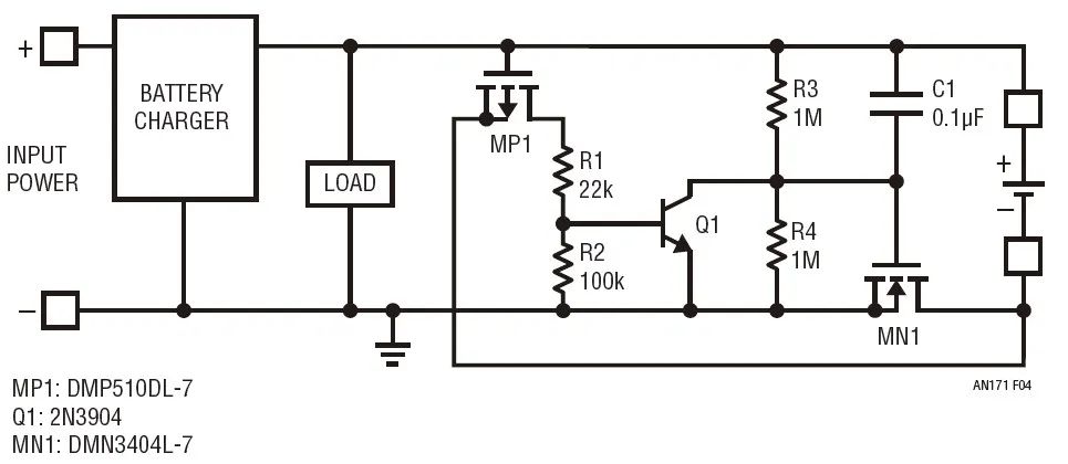
Figure 4: a practical reverse-battery circuit
However, using a small transmission transistor adds series impedance that lengthens the constant-voltage charging phase. For example, if the battery and wiring present 100 mΩ equivalent series resistance and a 100 mΩ isolation transistor is used, the constant-voltage charge phase time will double.
The MP1 and Q1 detection and disable network need not be extremely fast. Although MN1 dissipates high power during reverse-battery hot-plug, the disable circuit only needs to open MN1 before MN1 heats enough to be damaged. Tens of microseconds may be adequate. On the other hand, it is crucial to disable MN1 before the reversed battery can pull the charger and load voltages below ground, hence the need for C1. Essentially the circuit implements both an AC and a DC disable path.
This circuit was tested with a lead-acid battery and an LTC4015 battery charger. Figure 5 shows the charger OFF at reversed-battery hot-plug. The reversed voltage is not transferred to the charger or the load.
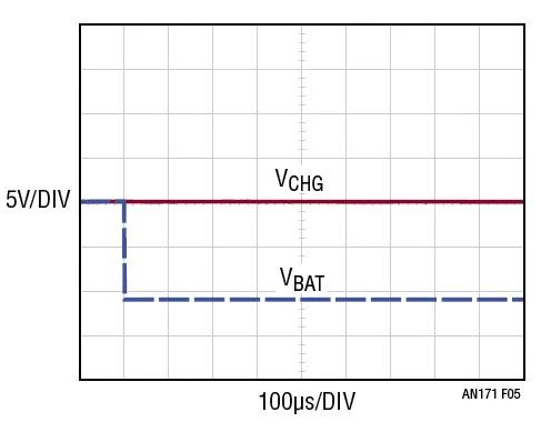
Figure 5: NMOS protection circuit with charger disabled
Note that MN1 must have a VDS rating equal to the battery voltage and a VGS rating equal to approximately half the battery voltage. MP1 must have VDS and VGS ratings equal to the battery voltage.
Figure 6 shows the more severe case when the charger is already running during reversed-battery hot-plug. The reversed battery pulls down the charger-side voltage until the detection and protection circuit disables the charger, allowing the charger to safely return to its regulated voltage. Dynamic behavior depends on the application, and the charger-side capacitance strongly affects the result. In this test the charger had both a high-Q ceramic capacitor and a lower-Q polymer capacitor.
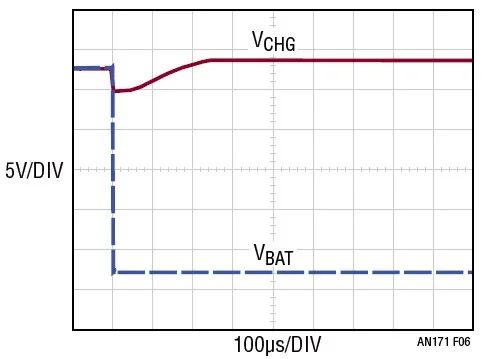
Figure 6: NMOS protection circuit with charger active
In general, using a polymer capacitor and an aluminum electrolytic capacitor on the charger improves behavior during normal forward-battery hot-plug. Pure ceramic capacitors can exhibit extreme nonlinearity and excessive overshoot during hot-plug because their capacitance can drop as much as 80% when voltage rises from 0 V to the rated voltage. This nonlinearity can create high inrush currents at low voltages and a rapid decrease in capacitance as voltage rises, a combination that can cause high voltage overshoot. Empirically, a ceramic capacitor paired with a lower-Q, voltage-stable aluminum or tantalum capacitor is a robust choice.
P-Channel MOSFET Design
The second method uses a PMOS transistor as the protection device, shown in Figure 7.
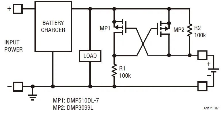
Figure 7: PMOS transistor transmission-element version
In this circuit, MP1 is the reverse-battery detector and MP2 is the reverse isolator. MP1 compares the battery positive terminal to the charger output by its source-to-gate voltage. If the charger terminal is higher than the battery, MP1 disables the main transmission device MP2. Thus, if the battery is driven below ground, MP1 will drive MP2 off by pulling MP2's gate toward its source. This behavior holds whether the charger is active and producing a regulated output or disabled at 0 V.
The main advantage is that MP2 inherently cannot pass negative voltage to the charger and load. Figure 8 illustrates this source-gate coupling effect.
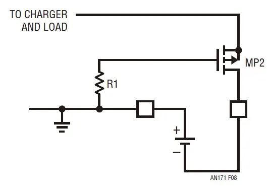
Figure 8: illustration of source-gate coupling effect
Through R1, the lowest gate voltage achievable on MP2 is 0 V. Even if MP2's drain is pulled far below ground, its source does not impose a substantial downward gate bias. As the source falls to a VTH above ground for the transistor, the device self-unbiases and its conduction falls. The closer the source approaches ground, the more the device bias is removed. This characteristic and the simple topology make this approach attractive compared to the NMOS method, although PMOS devices typically have lower conductivity and higher cost.
This circuit is simpler than the NMOS solution but has a significant drawback. Although it always provides reverse-voltage protection, it may not always connect the circuit to the battery. When the gates are cross-coupled as shown, the circuit forms a latch that can settle in the wrong state. Although it is difficult, a situation can occur where the charger is producing voltage (for example 12 V), a lower-voltage battery (for example 8 V) is attached, and the circuit remains open.
In that case MP1's source-to-gate voltage is +4 V, enhancing MP1 and disabling MP2. Figure 9 shows a possible stable-voltage node illustration for this blocking condition.
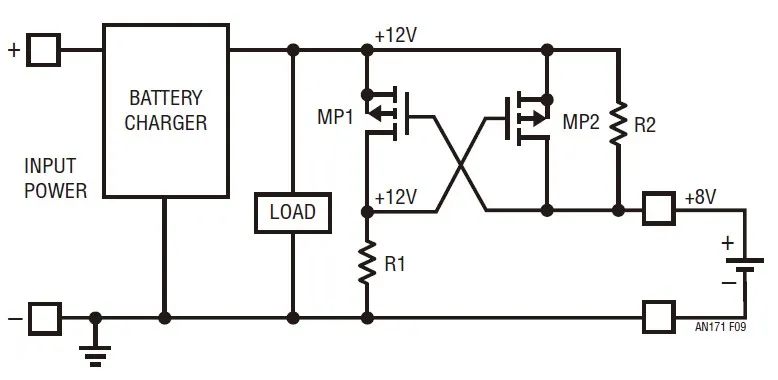
Figure 9: possible blocking state with PMOS protection
For this condition to occur the charger must already be active when the battery is attached. If the battery is present before the charger is enabled, MP1's gate is pulled by the battery and MP1 remains off. When the charger is later enabled it produces a controlled current rather than a large impulse, reducing the chance that MP1 will turn on and MP2 will turn off.
However, if the charger is active before the battery is attached, a transient voltage difference between the charger output and the battery terminal can cause MP1 to disable MP2 as the battery voltage is forced to absorb the charger capacitors' charge. This competition is between MP2's ability to draw charge from the charger capacitors and MP1's ability to disable MP2.
This PMOS circuit was tested with a lead-acid battery and an LTC4015 charger. Connecting a heavily loaded 6 V source as a battery simulator to an already-enabled charger never triggered the open state in these tests. The testing was not exhaustive and critical applications should be tested thoroughly. If the circuit does latch open, disabling and re-enabling the charger always reconnects the battery.
The failure state can be induced by applying a temporary connection between the top of R1 and the charger output, but generally the circuit tends to connect rather than block. If blocking becomes an issue, a design that disables the charger using additional devices can be implemented. Figure 12 provides a more complete example.
Figure 10 shows the PMOS protection circuit with the charger disabled.
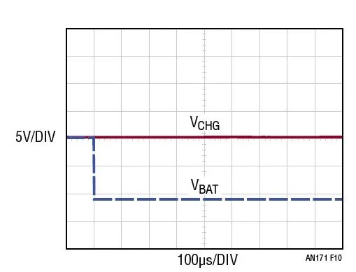
Figure 10: PMOS protection with charger disabled
Note that in all cases the charger and load voltages are not allowed to go negative.
Figure 11 shows the circuit in the adverse case where the charger is running during reversed-battery hot-plug.
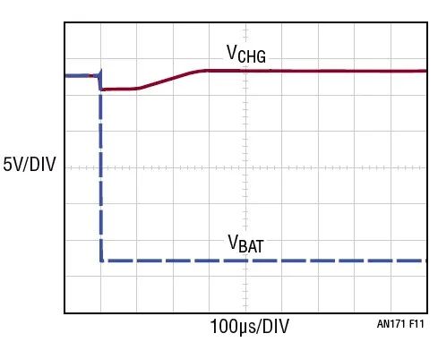
Figure 11: PMOS protection with charger active
As with the NMOS circuit, the reversed battery slightly drags down the charger and load voltages before the transmission transistor MP2 is driven off.
In this version MP2 must tolerate a VDS equal to twice the battery voltage (one from the charger and one from the reversed battery) and a VGS equal to the battery voltage. Conversely, MP1 must tolerate VDS equal to the battery voltage and VGS equal to twice the battery voltage. This requirement is unfortunate because MOSFETs are generally specified with VDS ratings above their VGS ratings. Transistors with 30 V VGS and 40 V VDS ratings are available for lead-acid applications. For higher-voltage batteries, additional zener diodes and series resistors are required to modify the circuit.
Higher-Voltage Example
Figure 12 shows an example that handles two series lead-acid batteries.
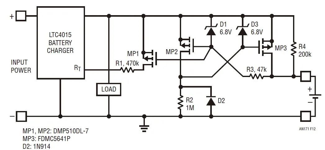
Figure 12: higher-voltage reverse-battery protection
D1, D3, and R3 protect the gates of MP2 and MP3 from excessive voltage. When a reversed battery is hot-plugged, D2 prevents MP3's gate and the charger output from quickly moving below ground. When the circuit detects a reversed battery or a latched-open error, MP1 and R1 detect the condition and use the missing LTC4015 RT signature to disable the charger.
Conclusion
Reverse-voltage protection circuits suitable for battery-charger systems can be developed. Several circuits were presented and briefly tested with encouraging results. There is no single magic solution to reversed-battery issues, but these approaches illustrate practical, low-cost options.
ADI states that the information provided is believed to be accurate. ADI assumes no responsibility for infringement of third-party patents or other rights that may result from use of the information. Specifications are subject to change without notice. No license to any ADI patents is implied or granted by the information.