Overview
This article explains why non-isolated DC-DC buck converters face significant challenges when converting a high DC input voltage to a very low output voltage at high output currents, and presents three compact approaches that achieve high step-down ratios while remaining space-efficient.
Design challenge
Designers can face the following challenge: converting a high DC input voltage to a very low output voltage (for example, from 60 V to 3.3 V at 3.5 A) while maintaining high efficiency, small size, and simple design. Combining a large input-to-output voltage difference with high current rules out linear regulators due to excessive power dissipation, so designers must use switching topologies. Even with a switching topology, achieving a compact layout for space-constrained applications is difficult.
Why buck converters struggle
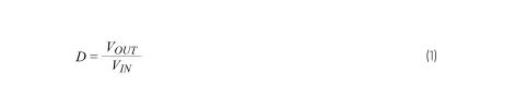
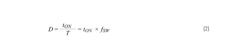
One option to achieve a high step-down ratio is a buck converter, because it can efficiently reduce a higher input voltage to a lower output voltage (for example, VIN = 12 V to VOUT = 3.3 V) while supplying substantial current in a small form factor. However, maintaining stable output regulation can be challenging under some conditions. For a buck converter operating in continuous conduction mode (CCM), the duty cycle D can be simplified as shown in the equation image below.
The relationship between duty cycle and switching frequency fSW is determined by the on-time tON, which is the time the control FET is on during each switching period T, as shown below.
Combining the two expressions shows how tON depends on the step-down ratio and fSW:
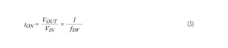
From this expression, when the VIN/VOUT ratio and/or fSW increase, tON decreases. That means the buck converter must operate with very short on-times to regulate output voltage under high VIN/VOUT ratios in CCM, which becomes harder at higher fSW. Consider an application with VIN(MAX) = 60 V, VOUT = 3.3 V, and IOUT(MAX) = 3.5 A. To evaluate the minimum required on-time tON(MIN), use VIN(MAX) and include the voltage drops across the two power MOSFETs, VSW(BOT) and VSW(TOP). Replacing VIN and including the MOSFET drops yields:
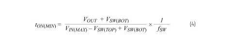
Using VIN(MAX) and fSW = 1 MHz in this expression gives tON(MIN) = 61 ns. To compute VSW(BOT) and VSW(TOP) we use RDS(ON)(BOT) and RDS(ON)(TOP) values from the LT8641 datasheet, with VSW(BOT) = RDS(ON)(BOT) × IOUT(MAX) and VSW(TOP) = RDS(ON)(TOP) × IOUT(MAX). The resulting minimum on-time of 61 ns is difficult for many buck converters to guarantee, so designers must consider alternate topologies. The following three practical solutions can achieve a high step-down ratio in a compact design.
Solution 1: Flyback with LT3748 (no optocoupler required)
The first option is an isolated topology: a transformer with an N:1 turns ratio handles most of the voltage step-down. ADI provides a flyback controller such as the LT3748 that does not require a third transformer winding or an optocoupler, simplifying the design and saving space. The LT3748 solution for this case is shown below.
Although the LT3748 approach simplifies the design relative to a standard flyback and reduces space, it still requires a transformer. For applications that do not need input-output isolation, avoiding the transformer will generally reduce complexity and overall size compared with isolated designs.
Solution 2: Two-stage step-down using LTM8073 and LTM4624 μModule devices
An alternative is to perform the step-down in two stages. Using two μModule devices plus eight external components, a compact solution with relatively few parts is possible. The LTM8073 and LTM4624 each integrate their power inductors, reducing a challenging layout and component-selection task. Both μModules use BGA packages (9 mm × 6.25 mm × 3.32 mm and 6.25 mm × 6.25 mm × 5.01 mm respectively), enabling a small footprint.
Under these conditions the LTM4624 shows 89% efficiency, and the LTM8073 can supply up to 1.1 A to the LTM4624 input. Because the LTM8073 can provide up to 3 A output current, it can power other rails as well. In the example shown below a 12 V intermediate voltage VINT is selected.
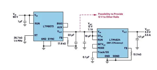
Although transformers are avoided, some designers may prefer not to use two separate buck converters, particularly if there is no need for the intermediate voltage to supply other rails.
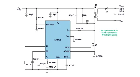
Solution 3: Single-stage buck using LT8641
In many cases a single buck converter is preferable because it can provide high system efficiency, small size, and simple design. Earlier we showed that many buck converters struggle with high VIN/VOUT and high fSW, but not all buck converters share the same limitations. The LT8641 from ADI has a short minimum on-time across its operating temperature range, typically 35 ns (maximum 50 ns). These specifications are below the previously calculated 61 ns minimum on-time, making the LT8641 a practical single-chip solution. The LT8641 circuit is simple, as shown below.
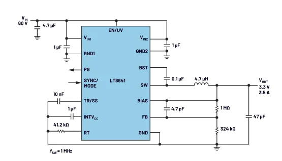
Note that the LT8641-based solution can also be the most efficient of the three options. If efficiency needs further optimization compared with the example in the figure, lowering fSW and choosing a larger inductor will improve efficiency. While a two-stage μModule solution can also reduce fSW, the integrated power inductors limit flexibility for further efficiency tuning beyond a certain point. Using two sequential step-down stages also has only a modest negative efficiency impact.
For the flyback solution running in boundary mode without an optocoupler, efficiency is high; however, transformer options restrict optimization. The LT8641 approach benefits from a wide range of available inductors, offering more flexibility for efficiency tuning.
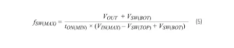
Confirming LT8641 suitability by rearranging the on-time equation
In most applications the only adjustable parameter in the minimum on-time equation is switching frequency. Rearranging the expression allows evaluation of the maximum allowable fSW for a given set of conditions. The rearranged formula appears in the LT8641 datasheet as well, and is shown below.
For the example VIN = 48 V, VOUT = 3.3 V, IOUT(MAX) = 1.5 A, and fSW = 2 MHz (48 V input is common in automotive and industrial applications), substituting into the expression gives:
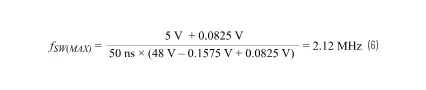
Therefore, under the given conditions the LT8641 can safely operate at switching frequencies up to 2.12 MHz, confirming it is suitable for this application.
Conclusion
This article presents three approaches to achieve compact designs for high step-down ratios. The LT3748 flyback solution eliminates the need for a bulky optocoupler and is appropriate when input-to-output isolation is required. The two-stage approach using LTM8073 and LTM4624 μModules is useful when designers want fewer components and integrated inductors or require an intermediate rail. The single-stage LT8641 solution offers a compact and simple option when a steep voltage step-down is needed and the minimum on-time requirements can be met.