Short-range wireless technologies power a vast array of modern electronics, from consumer devices and smart homes to industrial IoT, automotive systems, and medical equipment. The performance, reliability, and power efficiency of Bluetooth, Wi-Fi, Zigbee, NFC, UWB, and WiMAX depend heavily on the underlying printed circuit board. At Aivon, we specialize in manufacturing optimized RF PCBs that address the unique challenges of these protocols through precise impedance control, material selection, antenna integration, and EMI management.
This article explores these wireless standards from a PCB engineering perspective, highlighting design, layout, and manufacturing considerations critical for successful implementation.
Overview of Short-Range Wireless Protocols and PCB Implications
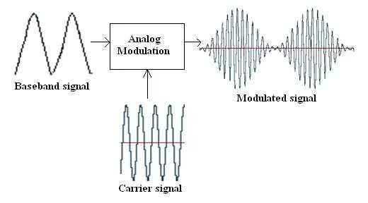
Each wireless technology operates with distinct frequency bands, data rates, power levels, and range requirements, directly influencing PCB architecture.
- Bluetooth: Low-power, short-range personal area networking with evolution from classic to BLE (Bluetooth Low Energy) and versions supporting audio, mesh, and high data rates.
- Wi-Fi: High-throughput local area networking, primarily in 2.4 GHz and 5 GHz bands (with 6 GHz in Wi-Fi 6E/7).
- Zigbee: Low-power, mesh networking ideal for sensor networks, operating mainly in the 2.4 GHz band.
- NFC: Very short-range (cm) communication at 13.56 MHz, used for secure identification and data exchange.
- UWB (Ultra-Wideband): High-precision ranging and positioning using wide bandwidth pulses.
- WiMAX: Longer-range broadband wireless, operating in licensed and unlicensed bands (historically 2-11 GHz).
Common PCB Challenges Across Protocols
Mixed-signal environments require careful separation of RF, digital, and power domains. Multilayer stack-ups with dedicated ground planes minimize crosstalk and provide low-impedance return paths essential for maintaining signal integrity.
Frequency Band Considerations and PCB Material Selection
The operating frequency heavily dictates PCB material and layout strategy.
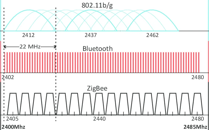
2.4 GHz Systems (Wi-Fi, Bluetooth, Zigbee)
This crowded ISM band demands excellent selectivity and interference rejection. PCB designs must minimize harmonic radiation and desensitization. Low-loss dielectrics help reduce insertion loss in filters and transmission lines.
5 GHz / 6 GHz Wi-Fi
Higher frequencies increase sensitivity to trace geometry variations and material losses. Rogers or high-performance FR4 laminates with stable Dk and low Df are preferred for maintaining consistent impedance and minimizing attenuation.
UWB (3.1-10.6 GHz)
Wide bandwidth requires broadband transmission lines with minimal dispersion and group delay variation. Tight impedance control and smooth copper surfaces are critical.
NFC (13.56 MHz)
Lower frequency allows more relaxed impedance requirements but demands careful loop antenna design and shielding to prevent coupling with nearby digital circuits.
PCB Material Strategies
High-Tg materials ensure thermal stability during sustained transmission. Hybrid stack-ups combine standard FR4 for digital sections with premium RF laminates for RF paths, balancing cost and performance.
Antenna Design and Integration on PCBs
Antenna performance is one of the most critical factors in wireless system success.
- Printed inverted-F antennas (PIFA), chip antennas, or PCB trace antennas are common for Bluetooth, Wi-Fi, and Zigbee.
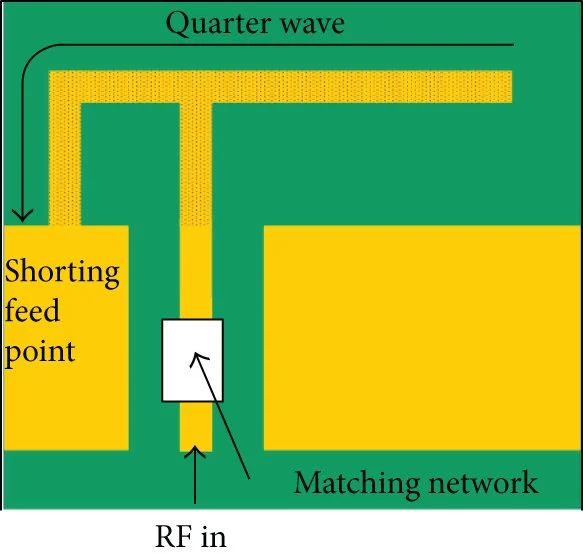
- NFC typically uses loop antennas integrated directly into the PCB layer.
- UWB benefits from specialized wideband antennas with consistent phase center.
Design Considerations:
- Keep-out zones and ground plane sizing significantly affect radiation efficiency and pattern. Multilayer boards often dedicate outer layers for antenna placement with continuous ground beneath the feed network.
- Diversity antennas for Wi-Fi and Bluetooth require isolation routing and switching networks with minimal parasitic effects.
- Impedance matching networks (pi or L networks) must be placed close to the antenna feed to compensate for enclosure and component loading effects.
RF Front-End and Power Management on Wireless PCBs
Modern single-chip solutions for Bluetooth and integrated Wi-Fi/Bluetooth combo modules reduce component count but increase layout density.
Key PCB Requirements:
- Power amplifiers in Wi-Fi and Bluetooth transmitters generate heat. Thermal vias, copper pours, and metal-core options help dissipate heat while preventing thermal drift in receivers.
- Low-noise power supplies are essential. LDOs and careful PDN design near RF transceivers preserve sensitivity and reduce phase noise.
- Front-end modules (FEMs) containing PAs, LNAs, and switches demand short, impedance-controlled traces between the SoC and antenna to minimize loss.
For WiMAX and higher-power applications, thicker copper layers and enhanced thermal management become even more important.
EMI/EMC, Signal Integrity, and Reliability Challenges
Coexistence is a major issue in devices supporting multiple protocols (e.g., Wi-Fi + Bluetooth + Zigbee).
Mitigation Techniques:
- Via fencing, ground stitching, and shielding cans isolate sensitive RF sections from digital noise.
- Careful clock routing and spread-spectrum techniques reduce peak emissions.
- For indoor positioning applications using UWB, precise time-of-flight measurements require ultra-low jitter clock distribution and matched trace lengths.
Manufacturing Considerations:
- Tight impedance tolerances (plus or minus 5-10%) and controlled etching are vital for consistent RF performance.
- HDI technology with microvias supports dense integration of single-chip wireless solutions.
- Enhanced reliability features like filled vias and robust solder mask prevent failures under thermal cycling and vibration common in automotive and industrial deployments.
PCB Manufacturing Best Practices for Wireless Devices
Successful production of multi-protocol wireless boards requires:
- Stack-Up Optimization: 6-12+ layers with balanced construction and multiple ground planes for EMI shielding.
- Fabrication Precision: Laser drilling, back-drilled vias, and via-in-pad for high-density RF layouts.
- Surface Finish: ENIG or ENEPIG for reliable RF connector and antenna pad performance.
- Testing: Vector Network Analyzer (VNA) measurements for impedance and antenna return loss, plus conducted and radiated emissions testing.
These practices support applications across consumer electronics, smart buildings, automotive connectivity, industrial automation, and healthcare devices.
Conclusion
Whether implementing low-power Zigbee sensor networks, high-throughput Wi-Fi, precise UWB positioning, or secure NFC transactions, the PCB serves as the foundation for wireless performance. Expert attention to material selection, impedance control, thermal design, antenna integration, and EMI management determines real-world range, data rate, power efficiency, and reliability.
At Aivon, our advanced PCB manufacturing capabilities help electronics engineers overcome the challenges of today's diverse short-range wireless technologies. From prototype to high-volume production, we deliver boards optimized for Bluetooth, Wi-Fi, NFC, UWB, and other protocols, ensuring your wireless products meet stringent performance and reliability requirements.