1.1 Background
RFID is increasingly used in industrial environments including automotive plants, garment and footwear factories, and logistics and warehousing. IO-Link interfaces are widely used in smart factories because of their generality and bidirectional data capabilities. STMicroelectronics' industrial automation group developed an IO-Link compatible RFID reader reference solution.
1.2 System Design
The IO-Link RFID sensor reference uses the L6364 and an STM32G0-based circuit to support IO-Link protocol conversion, and the ST25R3916 as the NFC/RFID reader IC. STMicroelectronics provides reference schematics, PCB designs, user guides, and software resources. The ST IO-Link slave protocol stack for slave devices is available for use with the L6364 combined with STM32G0, L0, or L4 series MCUs.
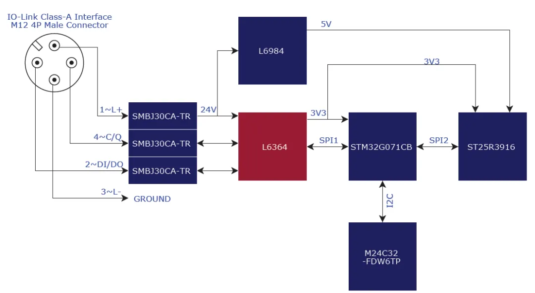
Figure 2. Block diagram
2 Hardware Design and Debugging
2.1 Reference Design
The product appearance is shown below. Reference schematics, PCB layouts, and related firmware are available from STMicroelectronics.
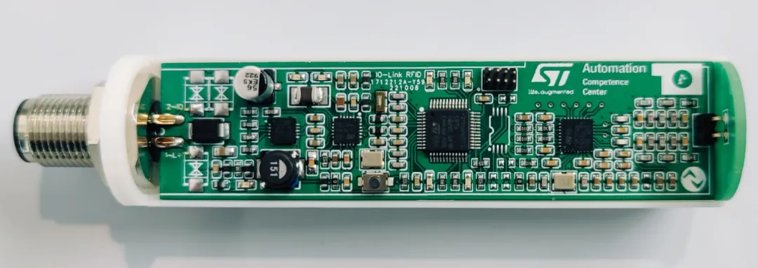
Figure 3. Hardware appearance
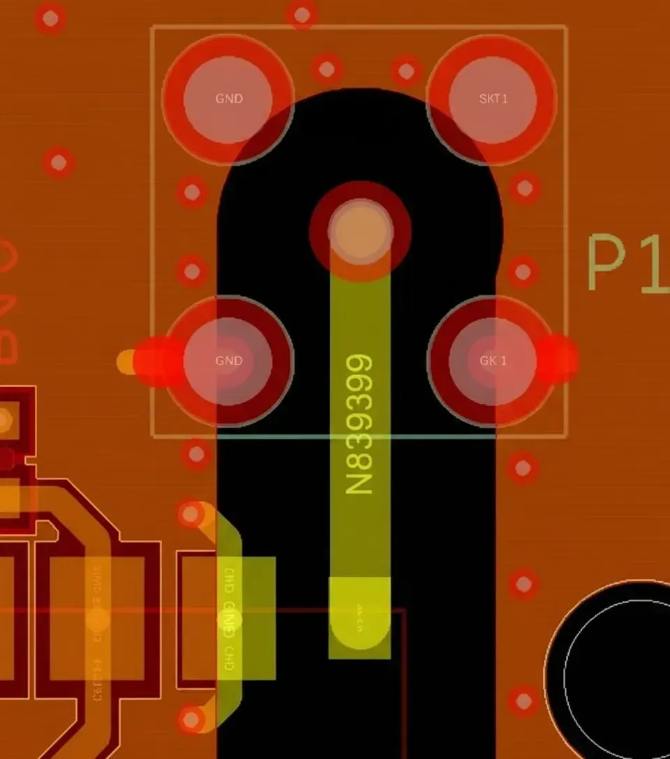
2.2 Antenna Design and Network Simulation Tools
In some applications such as automotive parts production lines and paint shop identification, the reader may need to operate at longer ranges, which raises requirements for RFID read/write performance. To increase read range, a larger antenna and improved impedance matching are typically required.
When a larger detection distance is needed, antenna size can be increased. Design tools are commonly used to assist antenna layout and simulation.
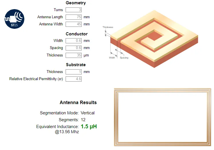
Figure 4. Antenna design
2.3 Antenna Impedance Matching and Simulation Tools
To achieve good antenna impedance matching and desired power output, use simulation tools to calculate matching network component values and evaluate performance.
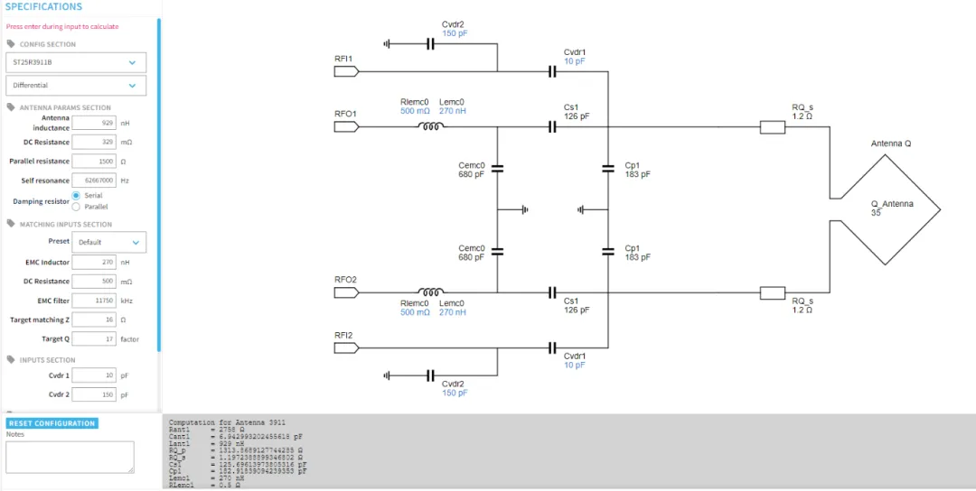
Figure 5. Antenna matching simulation