RF antenna integration on printed circuit boards has become essential as wireless connectivity proliferates across consumer, industrial, and automotive products. Effective antenna performance depends on both electromagnetic design and the physical realization of the PCB, where layout geometry, material properties, and fabrication precision directly influence radiation efficiency, impedance matching, and isolation from other circuits.
RF Antenna Design Fundamentals
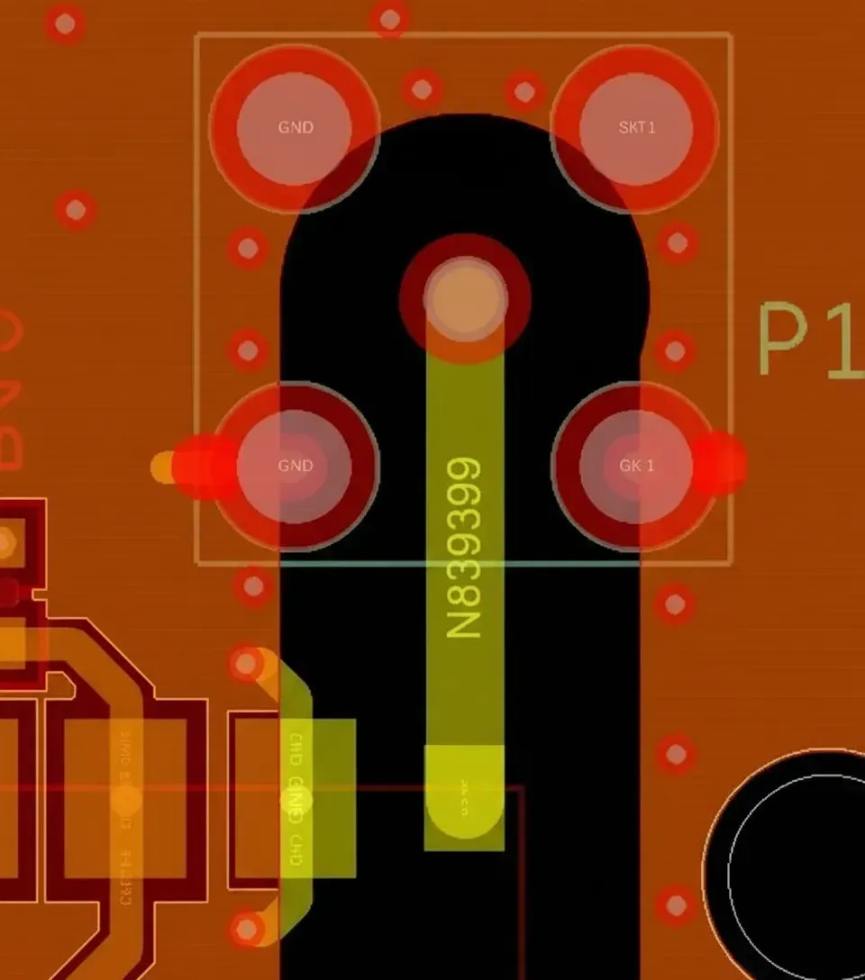
A typical PCB-mounted antenna comprises four functional elements: a radiating conductor that launches electromagnetic energy, a reference structure (often a ground plane) that shapes the radiation pattern, a feedline that delivers the RF signal from the transceiver, and an impedance-matching network that transforms the antenna's typically low impedance (commonly near 10 Ω) to the characteristic impedance of the feedline, usually 50 Ω. Proper matching minimizes reflections and maximizes power transfer within the target bandwidth.
Standard antenna topologies—planar inverted-F, patch, monopole, or printed dipole—are documented in microwave references and available as commercial off-the-shelf components. Regardless of topology, placement on the PCB must prevent the radiating element from being absorbed or detuned by nearby conductors, vias, or dielectric variations.
Layout Techniques for Isolation and Signal Integrity
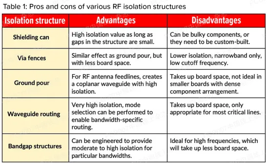
Two core layout strategies address the competing requirements of effective radiation, inter-circuit isolation, and electromagnetic compatibility.
First, functional blocks should be physically separated. Positioning the antenna near the board edge, distant from digital and analog sections, confines strong fields and reduces crosstalk. Continuous ground planes beneath the antenna and feedline maintain consistent return paths and minimize discontinuities that cause radiation or noise coupling. Field solvers integrated in modern PCB tools can identify return-path deviations early in layout.
Second, the antenna region itself is isolated through shielding structures, ground stitching, and controlled via placement. These measures block propagation between transmitters, receivers, and sensitive analog circuits. Electromagnetic simulation—preferably using finite-element methods—quantifies the trade-offs between isolation depth, feedline integrity, and antenna impedance before fabrication.
Applications and System Integration
RF antennas appear in smartphones, IoT modules, wireless sensors, automotive telematics, and industrial gateways. In mixed-signal boards, multiple antennas often coexist with high-speed digital buses and sensitive analog front-ends. Layout practices that maintain isolation become critical when simultaneous operation of Wi-Fi, Bluetooth, cellular, and GNSS is required.
Manufacturing Challenges
Fabricating PCBs that carry RF antennas introduces several precision requirements. Etch tolerance directly affects trace width and gap dimensions that define characteristic impedance. Copper surface roughness influences conductor loss at microwave frequencies. Dielectric thickness and permittivity must remain uniform across the panel to avoid detuning. Via placement and plating quality influence ground inductance and shielding effectiveness. For designs using flexible substrates, additional constraints arise from bending radius, copper ductility, and coverlay registration.
Environmental qualification—thermal cycling, humidity, vibration, and salt-fog exposure—further tests the mechanical and electrical stability of antenna structures and matching networks.
Materials and PCB/FPC Relevance
Material selection governs both radiation efficiency and manufacturing yield. Low-loss dielectrics such as PTFE, hydrocarbon ceramics, or specialized high-frequency laminates minimize insertion loss and maintain stable dielectric constant across temperature and frequency. Copper foil type (rolled versus electrodeposited) and surface roughness are chosen to balance skin-effect loss against cost and etchability. Flexible printed circuits enable compact, conformable antenna elements or interconnects between rigid sections and moving mechanical assemblies. High-density interconnect techniques support fine-pitch feedlines and dense via stitching for improved isolation. Thermal management layers or metal-core constructions can be incorporated when power amplifiers are co-located with antennas.
These material and stack-up decisions must be validated through impedance testing, S-parameter measurements, and near-field scanning during prototype stages.
Industry Trends
The rollout of 5G, Wi-Fi 6/7, and emerging 6G bands drives antennas toward millimeter-wave frequencies, wider bandwidths, and massive MIMO configurations. Multi-antenna systems increase the density of isolation structures and the importance of phase-matched feed networks. Integration with system-on-package and antenna-in-package technologies shifts some design responsibility to the PCB fabricator while demanding tighter collaboration on material properties and process controls.
PCB and Electronic Manufacturing Relevance
PCB fabrication and assembly processes are fundamental to realizing RF antenna performance. Controlled-impedance etching, laser-drilled microvias, sequential lamination, and precise surface finishes enable the transmission-line geometries and shielding structures required for low-loss feedlines and effective isolation. Automated optical inspection and electrical test verify trace dimensions and continuity before shipment. For flexible circuits, specialized handling and coverlay application maintain antenna integrity under mechanical flexure. These manufacturing disciplines allow electronics suppliers to deliver boards that meet the stringent signal-integrity, isolation, and environmental requirements of modern wireless products.
Conclusion
RF antenna design on PCBs combines electromagnetic principles with exacting layout and material choices. Separation of functional blocks, targeted isolation structures, and low-loss substrates are essential for maintaining radiation efficiency and signal integrity. The precision achievable in PCB fabrication—through controlled etching, dielectric uniformity, and advanced via technology—directly determines whether theoretical antenna performance is realized in production hardware. As wireless systems continue to integrate more antennas at higher frequencies, the partnership between RF design and high-reliability PCB manufacturing becomes increasingly critical for overall system success.