Radar systems are essential in automotive safety, aerospace, defense, industrial automation, and maritime navigation. Their performance in detection range, resolution, and interference resistance depends critically on the underlying printed circuit board. At Aivon, we specialize in manufacturing high-reliability RF PCBs that support complex radar applications through optimized high-frequency materials, precise impedance control, advanced thermal management, and multilayer integration.
This article examines radar antenna principles, system architectures, passive receivers, low probability of intercept (LPI) techniques, space-time adaptive processing, and anti-stealth strategies from a PCB engineering viewpoint.
Radar Antenna Types and PCB Integration Challenges
Radar antennas determine beam formation, gain, and scanning capability. Common types include parabolic reflectors, phased arrays, slotted waveguides, and microstrip patch arrays.
PCB Design Considerations:
- Phased Array Antennas: Widely used for electronic beam steering. These require dense integration of numerous RF channels on the PCB, with precise phase and amplitude matching across elements. HDI technology with microvias and tight trace length matching is essential to maintain beam accuracy.
- Patch and Printed Arrays: Often implemented directly on multilayer PCBs. Substrate dielectric constant (Dk) stability and low dissipation factor (Df) materials are critical to preserve resonance and minimize losses at operating frequencies (S-band to Ka-band and beyond).
- Feed Networks: Corporate or series feeds demand controlled impedance routing and minimal discontinuities. Back-drilled vias and smooth copper surfaces reduce insertion loss and phase errors.
Antenna integration on the PCB must account for radome effects, ground plane size, and nearby circuitry to prevent pattern distortion and maintain high gain.
Radar System Architectures and PCB Implementation
Modern radar systems employ various architectures: monostatic, bistatic, multistatic, and MIMO configurations.
Key PCB Requirements:
- Multichannel Transceivers: High-speed ADCs, DACs, and FPGA/DSP processors for waveform generation and signal processing require wide data buses with rigorous length tuning and dedicated power/ground planes to preserve signal integrity.
- Power Distribution: Pulse and continuous-wave radars create high transient currents. Robust PDNs with thick copper layers, multiple decoupling stages, and low-noise regulators prevent voltage droops that degrade transmitter performance.
- Thermal Management: High-power amplifiers and digital processors generate significant heat. Solutions include heavy copper planes, thermal vias arrays, embedded copper coins, and metal-core substrates to maintain component reliability under sustained operation.
Passive Radar Receivers and PCB Design
Passive radar systems detect targets by exploiting ambient illuminators (e.g., broadcast signals) rather than transmitting their own energy. They require highly sensitive, low-noise receiver chains.
PCB Considerations:
- Low-Noise Front-Ends: LNAs and high-dynamic-range ADCs need excellent isolation from digital noise. Separate analog and digital ground planes with via fencing minimize coupling and preserve noise figure.
- Wideband Reception: Passive receivers often cover broad frequency ranges, demanding low-dispersion transmission lines and stable material properties across temperature variations.
- Signal Processing: Real-time correlation and cross-ambiguity function computation place heavy loads on onboard processors, requiring high-layer count PCBs with optimized high-speed routing.
Low Probability of Intercept (LPI) Radar Technologies
LPI radars minimize detectability by using low-power, spread-spectrum, frequency-agile, or noise-like waveforms.
PCB Engineering Challenges:
- Waveform Generation: Direct Digital Synthesis (DDS) and complex modulation demand ultra-low jitter clocks and precise distribution networks to maintain phase noise performance.
- Fast Frequency Hopping: Requires broadband RF paths with consistent impedance and minimal group delay variation. Low-loss laminates and precision fabrication are vital.
- Power Management: Variable output power levels need efficient, fast-response DC-DC converters and careful layout to avoid spectral spurs that could compromise LPI characteristics.
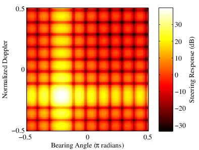
Airborne Radar and Space-Time Adaptive Processing (STAP)
Airborne platforms face severe constraints on size, weight, power, and vibration while managing clutter and jamming through STAP algorithms.
PCB Implications:
- Compact, Lightweight Designs: Rigid-flex and HDI constructions reduce overall system volume while supporting high channel counts for STAP processing.
- High-Throughput Processing: Real-time adaptive filtering requires substantial FPGA resources and high-bandwidth memory interfaces, supported by multilayer stack-ups with dedicated power planes.
- Reliability Under Stress: Vibration and thermal cycling in airborne environments demand robust via filling, high-Tg materials, and enhanced solder joint reliability to prevent failures.
Low-Frequency Anti-Stealth Radar Systems
Low-frequency radars (VHF/UHF) counter stealth technologies by exploiting resonance effects and reduced stealth material effectiveness at longer wavelengths.
PCB Design Considerations:
- Large Antenna Arrays: Lower frequencies allow physically larger elements but still require precise PCB-based feed networks and beamforming circuitry.
- High-Power Handling: Transmitters often operate at higher power levels, necessitating thick copper traces, wide power planes, and advanced thermal solutions.
- Interference Management: These bands are crowded, requiring sharp filtering and high dynamic range receivers. PCB-level isolation and shielding are critical to maintain sensitivity.
PCB Manufacturing Strategies for Radar Applications
Successful radar PCB production demands:
- Material Selection: Rogers, Taconic, or high-performance hybrid laminates with stable electrical properties across wide frequency and temperature ranges.
- Stack-Up Optimization: 8-24+ layer balanced constructions with multiple ground planes for shielding, power integrity, and EMI/EMC compliance.
- Fabrication Precision: Tight impedance tolerances, laser-drilled microvias, via-in-pad, and back-drilling to minimize discontinuities in RF paths.
- Thermal Solutions: Copper balancing, embedded heat spreaders, and coin technology for high-power RF sections.
- Reliability Enhancements: Filled and stacked vias, controlled CTE materials, and rigorous testing (VNA, TDR, thermal cycling) to ensure long-term performance in mission-critical systems.
These capabilities support applications in automotive ADAS radar, airborne surveillance, ground-based defense systems, and industrial collision avoidance.
Conclusion
Radar technology places some of the most demanding requirements on PCB design and manufacturing. From antenna array integration and multichannel architectures to LPI waveform handling and anti-stealth processing, every aspect of system performance traces back to signal integrity, thermal dissipation, material stability, and fabrication precision.
At Aivon, our expertise in advanced RF and high-reliability PCB manufacturing helps engineers overcome these challenges. By partnering early with an experienced manufacturer, radar system developers can ensure their designs achieve the necessary range, resolution, and robustness for today's complex operational environments.