Radio Frequency (RF) technology enables modern wireless communication, from 5G infrastructure and IoT devices to radar, satellite systems, and industrial automation. Successful RF implementation depends heavily on the underlying printed circuit board, where signal integrity, impedance control, EMI management, and material performance determine system reliability and range. At Aivon, we specialize in manufacturing advanced RF PCBs that translate these principles into production-ready solutions with precise fabrication and rigorous testing.
This article explores core RF concepts through a PCB engineering lens, covering frequency fundamentals, measurement units, key metrics, performance factors, and practical design considerations.
Understanding Radio Frequency: From Fundamentals to PCB Implementation
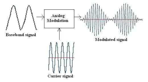
Radio Frequency refers to electromagnetic waves typically ranging from 3 kHz to 300 GHz. These signals carry information through modulation of amplitude, frequency, or phase.
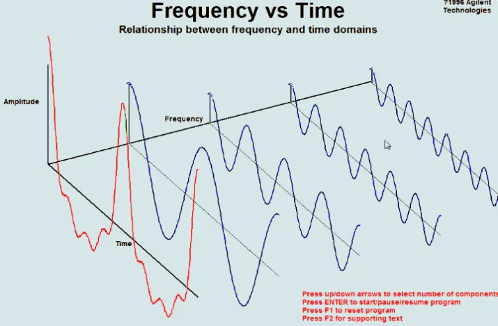
Frequency and Time Domain Relationship
RF signals are easier to analyze in the frequency domain (spectrum analysis) for identifying carriers, harmonics, and interference, while the time domain reveals transient behavior, modulation quality, and signal distortion. High-speed digital circuits on PCBs often generate RF-like noise that couples into sensitive analog sections. Converting between domains (via Fourier transforms) is essential during simulation and debugging.
PCB Implications:
High-frequency designs require careful stack-up planning with low-loss dielectrics (e.g., Rogers RO4000 series or high-performance FR4) to minimize insertion loss and dispersion. Controlled impedance traces (50 ohms standard for RF) and smooth copper surfaces (low-profile foil) become critical above 1 GHz.
Essential RF Units and Measurements for PCB Designers
Accurate power and signal level measurements use logarithmic units for wide dynamic ranges:
- dB (Decibel): Relative ratio between two power or voltage levels.
- dBm: Absolute power referenced to 1 milliwatt.
- dBW: Absolute power referenced to 1 watt (30 dB higher than dBm).
These units help quantify gain, loss, and power budgets across the RF chain - from antenna to transceiver.
PCB Design Relevance:
Link budget calculations directly influence trace width, via transitions, and connector selection. Excessive insertion loss from poor manufacturing (e.g., inconsistent dielectric thickness or rough copper) quickly degrades dBm levels at the receiver. Precision etching and impedance testing during fabrication ensure predictable performance.
Key RF Metrics: SNR, CNR, and System Performance Indicators
Several metrics define RF signal quality:
- Signal-to-Noise Ratio (SNR): Measures desired signal strength against background noise. Critical for digital modulation accuracy.

- Carrier-to-Noise Ratio (CNR): Focuses specifically on the carrier signal versus noise in analog or modulated systems. CNR is often more relevant in broadcast or satellite links, while SNR dominates in digital demodulation.
Other important metrics include phase noise, intermodulation distortion (IMD), spurious-free dynamic range (SFDR), error vector magnitude (EVM), and bit error rate (BER).
Real vs Ideal Signals in SDR Simulations
Software Defined Radio (SDR) tools often assume ideal conditions. In reality, component tolerances, thermal drift, phase jitter, and power supply noise create deviations that must be accounted for in PCB layouts.
PCB Considerations:
- Separate analog RF, digital, and power domains with strategic grounding and moats to preserve SNR/CNR.
- Use guarded traces, via fencing, and proper shielding cans to reduce crosstalk and external interference.
- Thermal stability affects phase noise and gain variation. High-Tg materials and thermal vias around RF amplifiers and oscillators maintain consistent performance across operating temperatures.
Key Factors Affecting RF System Performance on PCBs
Multiple elements influence overall RF effectiveness:
- Impedance Matching and Reflections: Mismatches cause signal loss and standing waves.
- Transmission Line Losses: Conductor, dielectric, and radiation losses increase with frequency.
- EMI/EMC and Crosstalk: Digital switching noise can corrupt sensitive RF receivers.
- Component Placement and Routing: Long traces or poor via transitions introduce inductance and parasitic effects.
- Power Supply Noise: Switching regulators can inject ripple that degrades CNR.
- Environmental Factors: Temperature, humidity, and vibration affect material properties and solder joint reliability.
Design Mitigation Strategies:
- Implement coplanar waveguides or microstrip/stripline topologies with reference planes.
- Minimize discontinuities using back-drilled or filled vias.
- Optimize PDN (Power Distribution Network) with multiple decoupling stages near RFICs.
- Choose materials with stable dielectric constants (Dk) and low dissipation factors (Df) for broadband performance.
PCB Manufacturing and Layout Best Practices for RF Applications
To achieve reliable RF performance, manufacturers must address:
- Material Selection: Low-loss laminates, controlled dielectric thickness, and hybrid constructions (RF + digital layers).
- Fabrication Precision: Tight impedance tolerance (plus or minus 5-10%), smooth copper profiles, and accurate registration for multilayer boards.
- Stack-Up Optimization: Dedicated RF layers with adjacent ground planes for shielding and return paths.
- Thermal Management: Copper pours, coin embedding, or metal-core options for high-power amplifiers.
- Testing and Validation: Vector Network Analyzer (VNA) measurements, time-domain reflectometry (TDR), and spectrum analysis on finished boards.
These techniques are vital across industries including 5G telecom infrastructure, automotive radar, industrial IoT sensors, medical wireless devices, and consumer wireless electronics.
Conclusion
Mastering radio frequency principles - from basic units and domain relationships to advanced metrics like SNR and CNR - is fundamental for successful wireless product development. However, the real-world performance ultimately depends on how effectively these principles are implemented at the PCB level through expert design and manufacturing.
At Aivon, we combine deep RF engineering knowledge with advanced fabrication capabilities to deliver PCBs that meet stringent wireless requirements for signal integrity, reliability, and manufacturability. Whether developing next-generation 5G systems, IoT edge devices, or specialized radar solutions, partnering with an experienced RF PCB manufacturer ensures your designs translate smoothly from simulation to high-volume production.