Introduction
In the sophisticated landscape of Surface Mount Technology (SMT), the solder paste printing process acts as the definitive gatekeeper of manufacturing quality. Industry statistics consistently reveal that approximately 60% to 70% of all soldering defects—including bridging, insufficient wetting, and solder balling—originate during the printing stage. At the epicenter of this critical process lies a precision-engineered tool: the SMT Stencil.
This comprehensive guide serves as a foundational resource for process engineers and PCB assembly managers. It synthesizes the essential elements of stencil technology, guiding you through the selection of mounting formats, the mathematics of aperture design, the kinetics of application, and strategies for both high-density assembly and precise rework.
Framed vs. Frameless Stencil Systems
Before delving into the microscopic details of aperture design, manufacturers must first address the macroscopic format of the stencil system. The physical configuration of the stencil—how it is tensioned and mounted—plays a pivotal role in storage logistics, cost efficiency, and print registration accuracy.
The Dynamics of Tension and Stability
The choice between framed and frameless systems is not merely a matter of cost; it is a trade-off between operational efficiency and process stability.
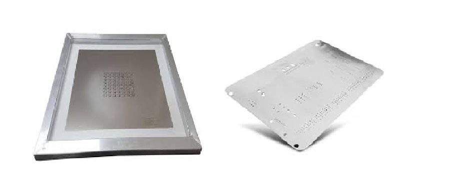
- Framed Stencils: In this traditional configuration, the stainless steel foil is permanently tensioned onto a rigid aluminum frame using a polyester mesh border. The primary advantage here is immediate stability. Because the tension is set by the stencil manufacturer, it remains consistent throughout the stencil's life. This "plug-and-play" nature makes framed stencils the preferred choice for high-volume, high-mix production lines where setup time must be minimized.
- Frameless Stencils: These systems utilize a reusable "universal frame" or tensioning master frame. The user purchases only the metal foil, which is mechanically tensioned into the master frame just before printing. The benefits are significant in terms of storage density and shipping costs. For facilities with limited warehousing, storing 500 foils in a filing cabinet is far more feasible than storing 500 aluminum frames.
Selecting the Right Format for Your Assembly Line
However, the decision extends beyond storage. Frameless systems require careful maintenance of the master frame to ensuring the tensioning mechanism does not degrade over time, which could lead to "smearing" or poor gasketing. Conversely, framed stencils, while bulkier, offer robust durability for heavy-duty cycling.
To analyze the cost-benefit ratio and operational impact of these systems in detail, read our comparative analysis: Framed vs. Frameless Stencils: Optimizing SMT Assembly for Quality and Efficiency
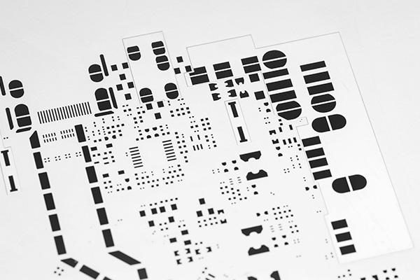
Optimizing Aperture Design
Once the stencil format is selected, the focus shifts to the core function of the tool: volumetrics. The primary goal of stencil design is not just to define where solder paste is deposited, but to control how much is deposited and ensure it releases cleanly from the foil.
The Mathematics of Release: Area and Aspect Ratios
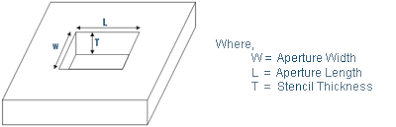
Solder paste is a thixotropic fluid—it changes viscosity under stress. For the paste to leave the stencil aperture and adhere to the PCB pad, the adhesive force between the paste and the pad must exceed the friction force of the aperture walls. This physics is governed by two critical industry standards (IPC-7525):
- Aspect Ratio (>1.5): The relationship between the aperture width (W) and the stencil foil thickness (T).
- Area Ratio (>0.66): The critical metric for modern fine-pitch assembly. It compares the area of the aperture opening to the surface area of the aperture walls.
Area Ratio = Area of Opening / Area of Walls
When the Area Ratio falls below 0.66, the paste tends to clog the aperture, leading to "insufficient solder" defects.
Geometric Modifications for Defect Prevention
Standard 1:1 aperture-to-pad designs are rarely sufficient for high-yield assembly. Engineers must employ geometric modifications to counteract material behavior:
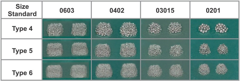
- Aperture Reduction: Typically, apertures are reduced by 10-15% relative to the pad size. This prevents "slump" (the spreading of paste after printing) from causing solder balls or bridging.
- Shape Optimization: Sharp corners in square apertures can trap paste. Rounding the corners (radius corners) or using "home plate" designs improves the release mechanism and reduces the frequency of under-stencil cleaning.
For a comprehensive look at how to calculate these ratios and modify geometries for specific component types, refer to: Optimizing Solder Paste Stencil Design for Flawless PCB Assembly
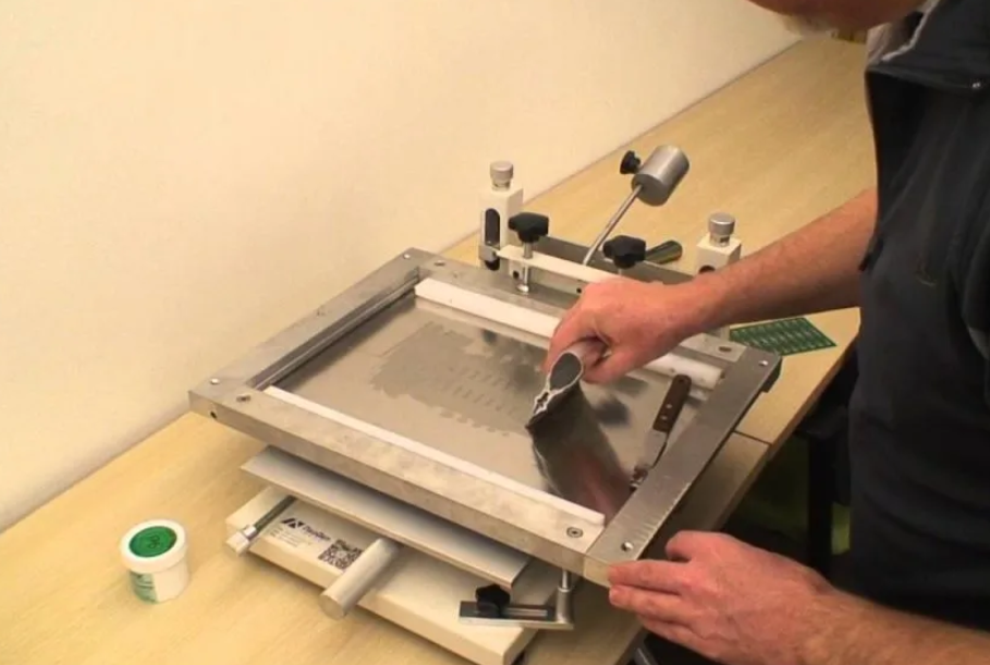
Mastering Squeegee Dynamics
A perfectly designed stencil is inert until acted upon by the squeegee. The squeegee is the engine of the printing process, responsible for rolling the paste to generate the hydraulic pressure necessary to fill the apertures.
Material Science: Metal vs. Polyurethane
The industry has largely transitioned from polyurethane (rubber) blades to stainless steel metal blades.
- The Problem with Polyurethane: Rubber blades are flexible. When they pass over a large aperture, they can dip inside, effectively "scooping" the paste out. This results in inconsistent deposit heights.
- The Metal Advantage: Metal blades maintain a rigid linear edge. They glide over the aperture, cutting the paste flush with the stencil surface. This is essential for maintaining a uniform brick profile across the entire PCB.
Critical Process Parameters
Controlling the squeegee requires balancing three interacting variables:
- Angle of Attack: typically set at 60 degrees. A lower angle increases downward pressure (pumping paste into holes), while a higher angle focuses on shearing.
- Speed: The speed determines the shear rate applied to the paste. If the speed is too high, the paste may slide rather than roll; if too low, cycle time suffers.
- Pressure: The "Goldilocks" zone is vital. Insufficient pressure leaves a film of paste on the stencil (smearing), while excessive pressure can "coin" (stretch) the stencil mesh and damage the foil.
Learn how to select the correct blade materials and tune your printer settings for optimal hydrodynamics in our article: Mastering Squeegee Choices for Flawless Solder Paste Application in PCB Assembly
The Frontier of Miniaturization: Fine-Pitch Stencils
As electronic designs shrink, manufacturers face the "Area Ratio Challenge." Components like 0.4mm pitch QFNs, µBGAs, and 01005 passives require thin stencils to ensure release, while large connectors on the same board require thick stencils for mechanical strength.
The Stepped Stencil Solution
To reconcile these opposing needs, Stepped Stencils (or Multi-Level Stencils) are employed:
- Step-Down: The foil thickness is locally reduced (etched or laser-milled) around fine-pitch components. For example, a 5-mil stencil might be stepped down to 4 mils for a µBGA, ensuring the Area Ratio remains healthy.
- Step-Up: Conversely, the foil can be locally thickened to deposit extra paste for through-hole reflow (THR) components or sturdy shield cans.
Nanocoatings and Material Enhancements
For ultra-high-density interconnect (HDI) applications, standard stainless steel may not suffice.
- Fine Grain Steel: Enhances the smoothness of laser-cut walls.
- Nanocoatings: These are hydrophobic/oleophobic treatments applied to the stencil. They repel flux and solder paste, significantly improving the definition of the printed "brick" and increasing the number of print cycles possible between cleaning intervals. This is a game-changer for maintaining yield on 0.3mm pitch devices.
Discover the specific strategies for overcoming the physical limits of miniaturization in our dedicated piece: Fine-Pitch SMT Stencils: Achieving Precision in High-Density PCB Assembly
Beyond Production: Stencils for Rework and Repair
Even in the most optimized environments, rework is a reality. When a BGA or QFN fails testing and needs replacement, the primary production stencil cannot be used. The challenge lies in replicating the precision of the original machine print during a manual repair process.
The Pitfalls of Manual Dispensing
Historically, technicians might use a syringe to dispense paste onto pads. However, this method is fraught with inconsistency. Dot sizes vary, leading to shorts (too much paste) or opens (too little paste), particularly on components where visual inspection of the joint is impossible (like BGAs).
The Role of Mini-Stencils
The professional solution is the Mini-Stencil (or Component-Specific Stencil). These are small, standalone metal foils cut with the exact same aperture design and thickness as the production stencil.
- Consistency: They ensure the replacement component sits on a paste deposit identical to the original manufacture.
- Tooling: They can be used with rework stations or simple manual taping methods, provided alignment is handled with care.
- Direct-Component Printing: In some scenarios, paste is printed directly onto the component balls rather than the PCB pads, a technique that requires specialized tooling fixtures.
To explore the techniques for maintaining reliability during the repair phase, read our guide on: SMT Stencils for Rework and Repair: Techniques and Considerations
Conclusion
The SMT stencil is not merely a sheet of metal with holes; it is the blueprint of assembly reliability. From the initial decision of using a Frameless system for flexibility, to the engineering rigor of Aperture Area Ratios, and the kinetic precision of Metal Squeegees, every variable interacts to define the final quality of the product.
By adhering to the principles outlined in this guide and the accompanying detailed articles, PCB assemblers can move from reactive defect correction to proactive process mastery, ensuring every solder joint meets the highest standards of electrical and mechanical integrity.