Component Alignment
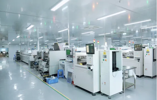
Component alignment plays a crucial role in the design and manufacturing of printed circuit boards (PCBs), ensuring that electronic components are precisely positioned for optimal performance and reliability. In PCB assembly, proper alignment minimizes issues such as soldering defects, signal interference, and mechanical stress, which can lead to failures in high-stakes applications like consumer electronics, automotive systems, or medical devices. For engineers and hobbyists searching for guidance on component alignment, this tag gathers resources that delve into techniques for achieving accurate placement, from manual adjustments in prototyping to automated processes in mass production. Understanding component alignment starts with fundamental principles, including the use of fiducial markers, which serve as reference points for pick-and-place machines to align components with sub-millimeter precision. Best practices include selecting appropriate board layouts that account for thermal expansion, component tolerances, and assembly line constraints. For instance, aligning surface-mount devices (SMDs) requires careful consideration of pad designs and stencil apertures to prevent tombstoning or bridging during reflow soldering. Articles under this tag offer practical insights, such as step-by-step tutorials on using software tools like KiCad or Altium Designer to verify alignment before fabrication, and troubleshooting tips for common misalignment problems that arise during wave soldering or manual assembly. By focusing on these actionable strategies, readers can enhance their PCB designs to meet industry standards like IPC-A-610, reducing rework costs and improving yield rates. Whether you are optimizing a new prototype or refining an existing production process, the content here provides valuable knowledge to address real-world challenges in electronics manufacturing. Browsing the related articles can help you apply these concepts effectively in your projects.
Video Guide
No videos found for this tag.
Technical Articles
Get in Touch
Send Message
- Products & Service
- Company
- About AIVON
- Contact
- News
- Blog
- Certification
-


- Payment
-


2026 AIVON.COM All Rights Reserved