Fine Pitch PCB
Fine pitch PCBs represent a critical advancement in printed circuit board design, enabling the integration of high-density components with lead spacings typically below 0.65mm, such as 0.5mm or 0.4mm. This technology is essential for modern electronics where space constraints demand miniaturization without sacrificing performance. Engineers and designers often seek information on fine pitch PCBs to address challenges like precise component placement, signal integrity, and thermal management in applications ranging from smartphones and wearables to automotive systems and medical devices. By understanding the fundamentals of fine pitch design, professionals can optimize layouts to reduce board size, improve electrical efficiency, and enhance overall device reliability. In practice, working with fine pitch PCBs requires adherence to best practices in manufacturing and assembly. For instance, selecting appropriate solder paste stencils with laser-cut apertures ensures accurate deposition, while advanced reflow soldering techniques minimize defects like bridging or tombstoning. Designers should also consider via-in-pad designs and controlled impedance traces to maintain signal quality in high-speed circuits. These approaches not only mitigate common pitfalls but also facilitate scalability for production runs. Articles tagged under Fine Pitch PCB delve into these topics, offering detailed guides on tools, materials, and troubleshooting methods that can directly inform your projects. For those troubleshooting assembly issues or exploring innovative layouts, the resources here provide actionable strategies drawn from industry expertise. Reviewing case studies on fine pitch implementation in real-world scenarios can help refine your techniques, whether you're prototyping a compact IoT device or upgrading legacy systems. This collection of content serves as a valuable reference for staying current with evolving standards in PCB technology.
Technical Articles
Why Your Solder Mask Bridge Keeps Failing – Real Spacing Limits from Production
How to Avoid Common Solder Mask & Stackup Issues in 6-Layer HDI PCBs
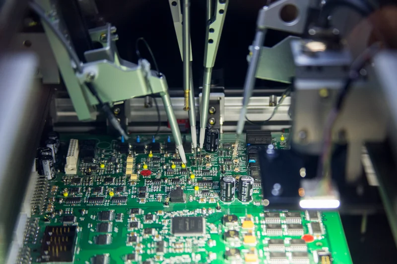
Challenges in using FPT
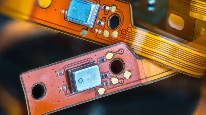
High Density Interconnect (HDI) Flexible PCBs: Maximizing Space and Performance
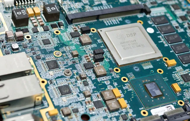
The Role of HDI PCBs in Telecommunication Base Stations: Benefits and Design Considerations
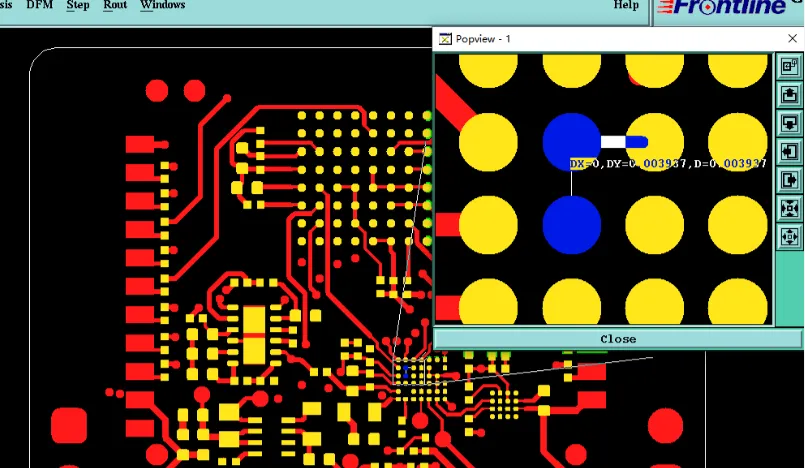
Engineering Case Study: 4-Layer 0.4mm Thin FR-4 PCB Tight BGA Solder Mask Bridge and Marking DFM Review
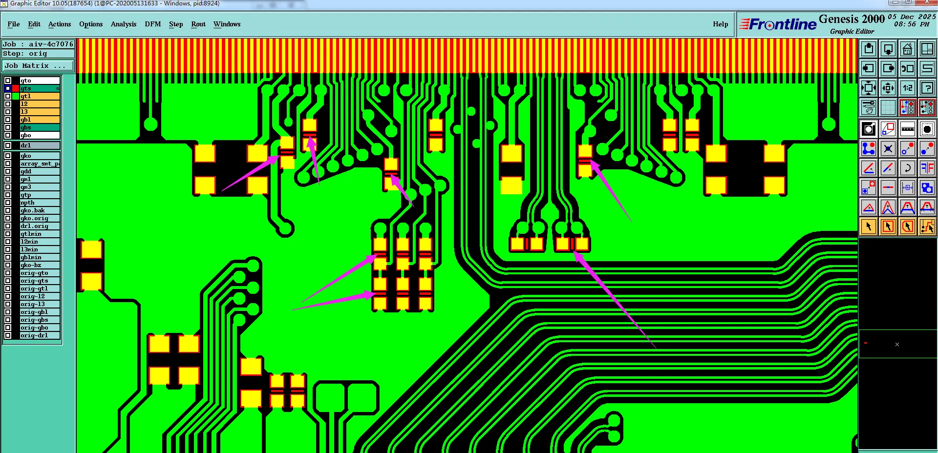
How DFM Prevented SMT Shorts from Narrow Mask Bridges
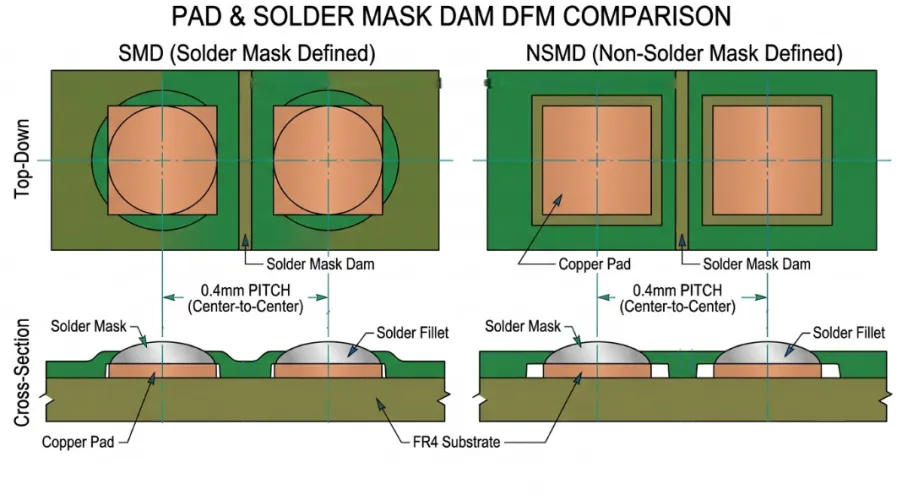
Why HDI PCB Designers Should Avoid Small Solder Mask Bridges
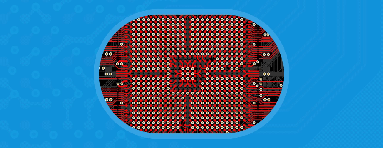
HDI BGA Fanout Design Mistakes That Cause Assembly Issues
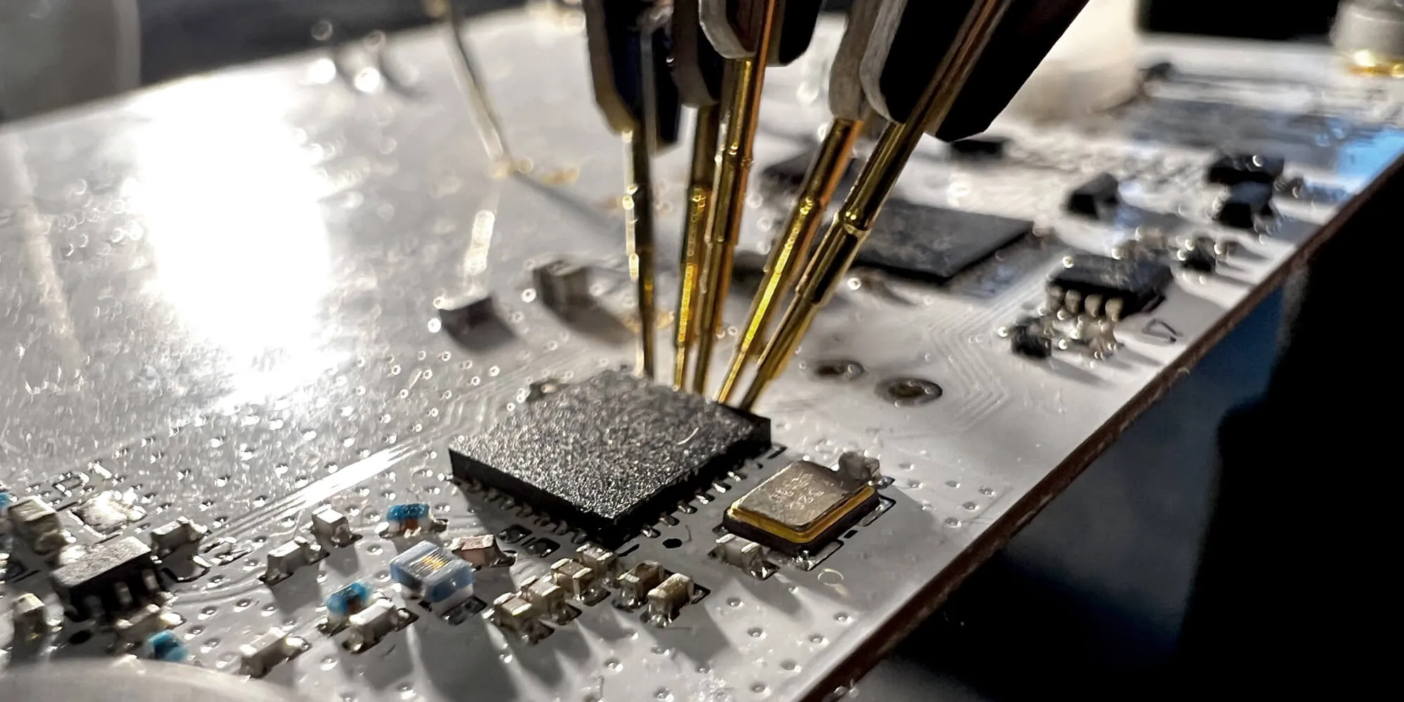
Selecting Test Probes for SMT PCBs: A Comprehensive Guide
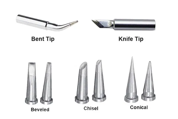
The Ultimate Guide to Choosing the Right Manual Soldering Station for SMD Rework

Precision Solder Paste Application: Mastering Stencil Printers for Fine Pitch PCBs
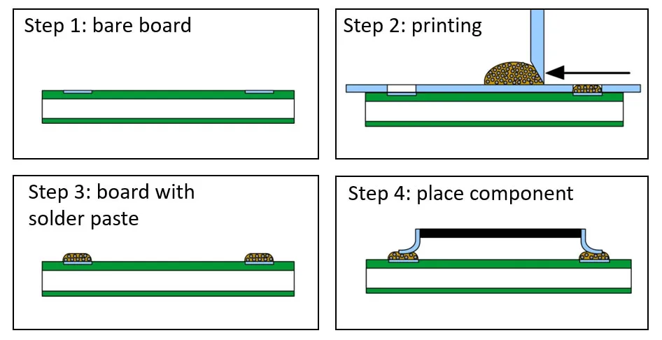
Advanced Stencil Printing Techniques: Achieving High Density SMT Assembly
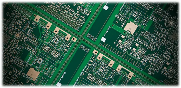
Silkscreen Design for High Density PCBs: Achieving Clarity in Compact Spaces
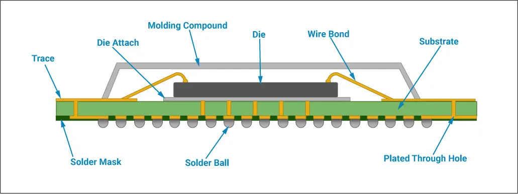
Choosing the Right PCB Substrate for Fine Pitch Component Assembly
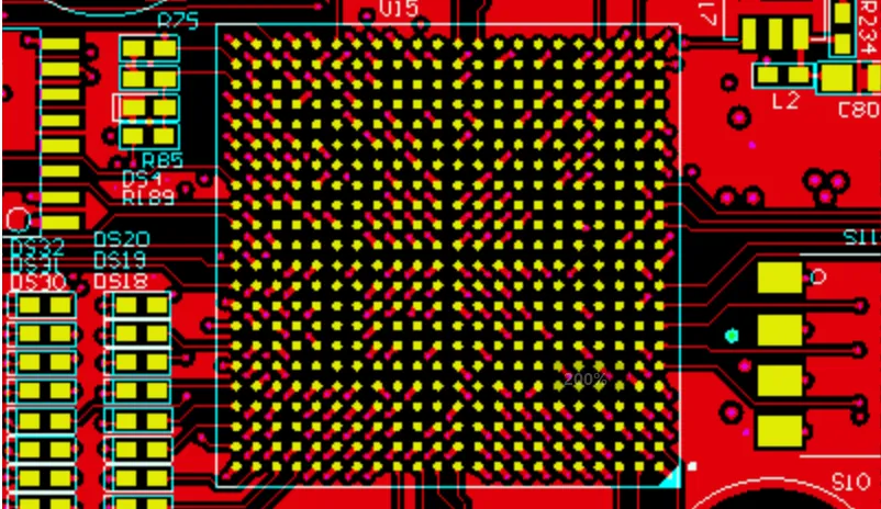
Fine Pitch Components: Achieving Optimal Pad to Pad Spacing for Reliable Connections
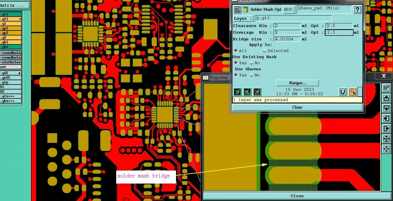
What is a Solder Mask Bridge in PCB Design?
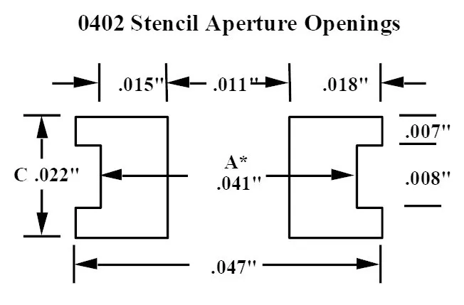
The Art of SMT Stencil Aperture Design: Minimizing Defects and Maximizing Yield