HDI PCB Etching
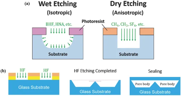
High-density interconnect (HDI) printed circuit boards represent a critical advancement in electronics design, enabling the creation of compact, high-performance devices with intricate multilayer structures. The process of HDI PCB etching plays a pivotal role in this technology, involving the precise removal of copper layers to form fine-pitch traces, vias, and pads that support advanced functionalities in smartphones, medical devices, and automotive systems. For engineers and manufacturers searching for insights on HDI PCB etching, this tag serves as a comprehensive resource, covering the fundamentals of chemical and laser etching methods, material considerations, and optimization strategies to achieve superior board density without compromising reliability. Understanding HDI PCB etching is essential for addressing common challenges such as maintaining signal integrity in high-speed applications or minimizing defects like over-etching and under-etching. Practical applications include designing boards with microvias and buried vias, where etching precision directly impacts yield rates and overall performance. Best practices emphasize selecting appropriate etchants, controlling process parameters like temperature and exposure time, and incorporating design for manufacturability (DFM) principles to reduce costs and improve scalability. By focusing on these elements, professionals can enhance their workflows, from prototyping to mass production, ensuring that HDI boards meet stringent industry standards for miniaturization and efficiency. This tag aggregates a range of articles that delve into specific etching techniques, case studies from real-world implementations, and troubleshooting guides for common issues. Readers interested in advancing their knowledge can find detailed explorations of related topics, such as via filling and plating processes that complement etching in HDI fabrication. Whether you are refining your manufacturing approach or seeking solutions to etching-related problems, the content here provides actionable guidance to support informed decision-making in PCB development.
Get in Touch
Send Message
- Products & Service
- Company
- About AIVON
- Contact
- News
- Blog
- Certification
-


- Payment
-


2026 AIVON.COM All Rights Reserved