Mounted Stencils
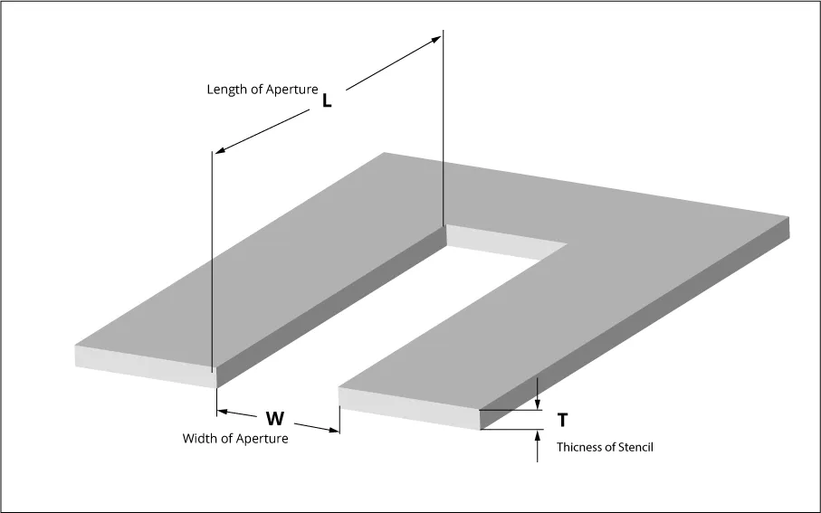
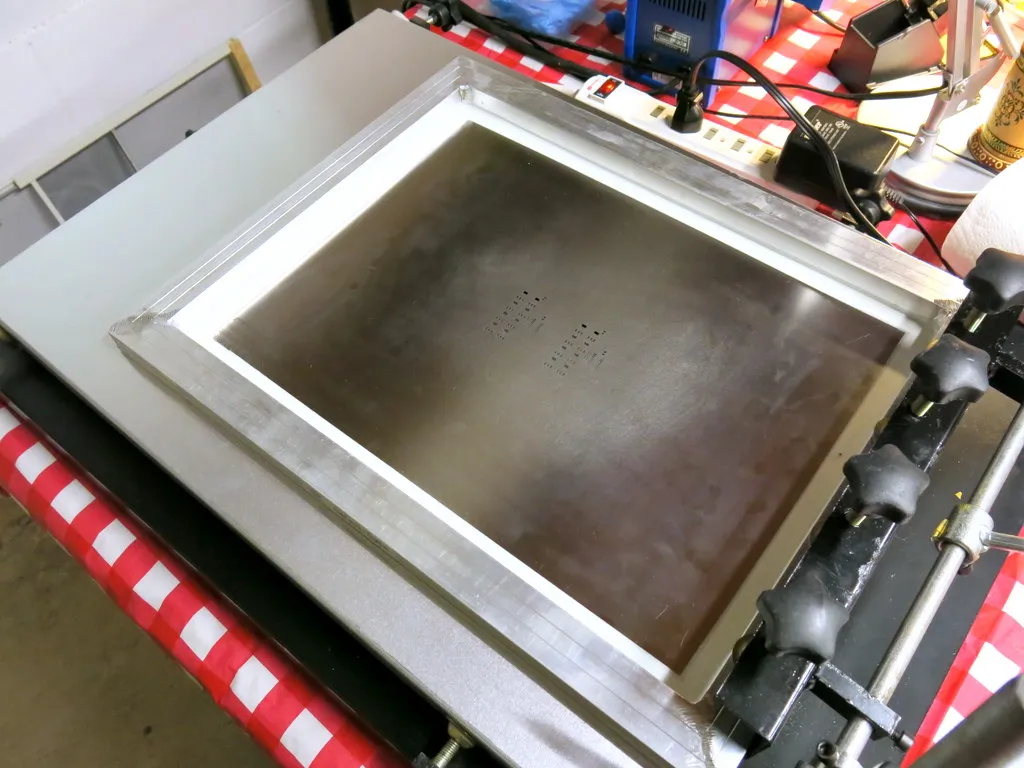
Mounted stencils play a crucial role in the precision assembly of printed circuit boards, serving as framed metal templates that ensure accurate application of solder paste during surface mount technology processes. These stencils are typically laser-cut from stainless steel and secured within a rigid frame, allowing for consistent alignment and repeatability in high-volume production environments. For engineers, hobbyists, and manufacturers searching for information on mounted stencils, this tag provides a centralized resource to understand their design, implementation, and optimization, helping to minimize defects such as bridging or insufficient paste deposition that can compromise PCB functionality. One of the primary advantages of mounted stencils lies in their stability and ease of use compared to frameless alternatives. They integrate seamlessly with automated stencil printers, enabling faster setup times and reduced operator error. In practical applications, selecting the right stencil thickness—often between 0.1mm and 0.2mm depending on component pitch—directly impacts solder joint quality. Best practices include regular cleaning with isopropyl alcohol to prevent aperture clogging and verifying aperture designs against Gerber files to match specific board layouts. By adhering to these guidelines, users can achieve higher first-pass yields and extend the lifespan of their stencils, ultimately lowering production costs. For those delving deeper into PCB fabrication, the articles under the Mounted Stencils tag offer in-depth explorations of topics like stencil tensioning techniques, material choices for different environmental conditions, and troubleshooting common issues in reflow soldering. Whether you are prototyping a new design or scaling up manufacturing, these resources equip you with the knowledge to enhance assembly efficiency and reliability.
Video Guide
No videos found for this tag.
Technical Articles
Get in Touch
Send Message
- Products & Service
- Company
- About AIVON
- Contact
- News
- Blog
- Certification
-


- Payment
-


2026 AIVON.COM All Rights Reserved