Introduction
In high-density PCB assembly, precise solder paste application sets the foundation for reliable component placement and soldering. Mounted stencils, which feature a thin metal foil stretched and secured on a rigid frame, enable consistent printing across large production runs. Engineers face unique challenges with fine pitch components, where even minor variations in paste deposition can lead to defects like bridging or insufficient solder joints. Selecting the appropriate mounted stencil involves balancing aperture design, material properties, and printing parameters to optimize solder paste volume. This guide draws on practical insights to help electrical engineers navigate these decisions, ensuring first-pass yields in demanding applications. By focusing on proven engineering principles, you can mitigate risks associated with high-density PCB stencils.
What Is a Mounted Stencil and Why It Matters for High-Density PCBs
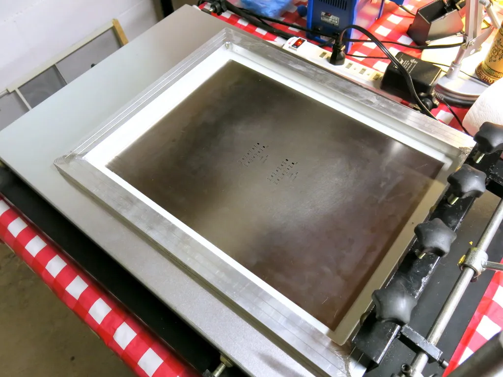
A mounted stencil consists of a precision-cut foil, typically stainless steel or nickel, tensioned onto a sturdy frame compatible with automated stencil printers. This design contrasts with frameless options by providing stable tension and repeatability, essential for high-volume surface mount technology processes. The foil features laser-etched or electroformed apertures that match the PCB pad layout, allowing controlled release of solder paste during printing. For high-density PCBs packed with small components like 01005 resistors or 0.3mm pitch BGAs, the mounted stencil becomes critical to achieve uniform paste volume without defects.
The relevance intensifies in modern electronics, where shrinking component sizes demand fine pitch stencils capable of handling apertures below 0.2mm. Poor stencil selection leads to issues such as paste starvation on small pads or bridging between closely spaced leads, compromising assembly reliability. Engineers must prioritize stencils that support precise control over solder paste volume, directly impacting reflow outcomes and long-term joint integrity. Industry standards like IPC-7525 outline guidelines for stencil fabrication to address these demands systematically.
Framed (Mounted) vs. Frameless Stencil Comparison
| Feature | Mounted (Framed) Stencil | Frameless Stencil | Best Use Case |
|---|---|---|---|
| Tension Stability | Excellent, factory-set | Variable, depends on printer/frame | High-volume production |
| Print Repeatability | Very high across 10,000+ prints | Good for low volume | Automated SMT lines |
| Cost per Unit | Higher initial cost | Lower | Prototyping & NPI |
| Setup Time | Minimal (drop-in ready) | Higher (requires tensioning) | High-mix, high-volume |
| Durability & Cleanings | Superior | Moderate | Fine-pitch, high-density boards |
| Suitability for HDI | Preferred | Acceptable only for prototypes | Complex, dense PCBs |
Key Technical Principles in Mounted Stencil Design
Stencil material selection influences durability, aperture quality, and paste release performance. Stainless steel foils offer robustness for repeated cleanings, while electroformed nickel provides smoother walls for better release in fine pitch applications. Laser cutting delivers sharp-edged apertures ideal for small component stencils, minimizing paste residue compared to chemical etching. Engineers evaluate these based on the smallest feature size on the board, ensuring the material withstands printer squeegee pressure without warping.
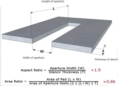
Aperture design governs solder paste volume and transfer efficiency, with shape and size tailored to pad geometry. Rectangular apertures suit most QFP leads, but U-shaped or scooped profiles enhance release for fine pitch stencils by reducing surface tension effects. The aspect ratio, defined as aperture length divided by foil thickness, must exceed typical industry thresholds like 0.66 to promote clean paste withdrawal. Similarly, area ratio considers aperture opening relative to wall contact area, guiding designs for high-density PCB stencils. These parameters prevent common failures in small component stencil printing. For a deeper dive into calculations and real-world application, see our stencil aspect ratio vs area ratio guide.
Foil thickness directly controls deposited paste volume, thinner profiles suiting fine pitch while thicker ones support larger components. For high-density assemblies, balancing thickness ensures adequate volume for joint formation without excess that causes bridging. Tensioning in mounted stencils maintains flatness, critical for gasket seal against the PCB surface. Variations in these principles can amplify defects during high-speed printing.
Practical Solutions and Best Practices for Selection
Start by analyzing the PCB layout to identify the finest pitch and smallest apertures required. Group components by pitch: use uniform thickness for similar fine pitch stencils, or consider multi-level designs for mixed sizes on high-density boards. Consult IPC-7525 for aperture reduction rules, typically shrinking openings slightly relative to pads to contain paste effectively. Validate designs through simulation or test prints to confirm solder paste volume matches reflow requirements.
Material and fabrication choices depend on production scale. Opt for laser-cut stainless steel in mounted stencils for prototypes transitioning to volume, as it balances cost and precision for small component stencils. Apply nano-coatings to apertures if release issues persist, reducing friction without altering base design. Frame size should match printer capabilities, with tension levels verified to avoid foil distortion.
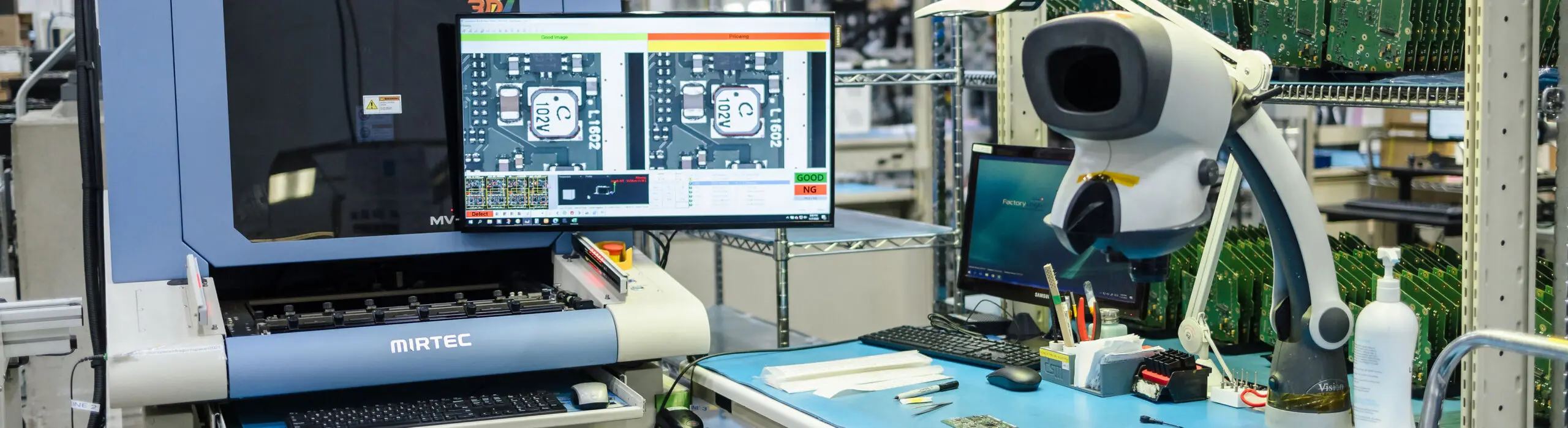
Printing parameters interact closely with stencil selection. Adjust squeegee speed and pressure to optimize gasketing for fine pitch stencils, starting with slower speeds to aid paste shear. Implement under-stencil cleaning regimes, such as every 5-10 prints, to sustain aperture integrity. Post-print inspection via SPI confirms solder paste volume uniformity across high-density regions.
- Foil Thickness: Thinner for fine pitch (<0.5mm) - Reduces bridging risk
- Aperture Shape: Scooped or trapezoidal - Improves paste release
- Material: Laser-cut stainless steel - Sharp edges for small features
- Tension: 20-30 N/cm typical - Ensures flatness and seal
- Coating: Nano-polymer - Enhances clean release
Material Comparison Table :
| Material | Aperture Wall Quality | Paste Release | Durability (Cleanings) | Cost | Best For |
|---|---|---|---|---|---|
| Laser-cut Stainless Steel | Good (slight taper) | Very Good | Excellent (>10,000) | Medium | Most high-density production |
| Electroformed Nickel | Excellent (straight, smooth) | Superior | Very Good | Higher | 0.3 mm pitch and below, critical applications |
Engineers often debate stainless steel versus electroformed nickel for high-density applications.
Troubleshooting Common Issues with Fine Pitch Stencils
Insufficient solder paste volume often stems from low area ratios in aperture design, starving small component joints and causing opens post-reflow. Increase aperture width or thin the foil, then retest transfer efficiency. Bridging plagues fine pitch stencils when excess paste volume flows between pads; solutions include tighter aperture-to-pad matching and optimized squeegee hardness. Verify printer alignment, as misalignment exacerbates this in high-density layouts.
Poor release leaves residue in apertures, disrupting subsequent prints. Switch to electroformed stencils or add wall polishing for smoother surfaces. Warpage in mounted stencils from improper tension leads to uneven gasketing; recalibrate frame tension and inspect foil flatness routinely. For persistent issues, reference IPC-A-610 criteria during visual and AOI checks to correlate stencil performance with assembly defects.
In mixed-technology boards, fine pitch stencils may underperform near larger apertures due to volume inconsistencies. Employ step-up stencils to vary thickness regionally, tailoring solder paste volume precisely. Document printer logs and paste rheology to isolate variables systematically.
Validation, SPI Inspection & Continuous Improvement
Solder Paste Inspection (SPI) is non-negotiable for high-density boards. Target ±10% volume tolerance on critical pads. Combine SPI data with AOI and X-ray results to build a closed-loop improvement process. Track key metrics: transfer efficiency, Cpk of paste volume, and defect rates per thousand opportunities (DPMO). Many manufacturers achieve >98% first-pass yield by iterating stencil designs based on SPI feedback.
Case Studies & Real-World Results
Medical Device Manufacturer (HDI Board with 0.3 mm Pitch BGAs)
Switching from a standard 0.127 mm stainless laser-cut stencil to a 0.10 mm electroformed nickel mounted stencil with nano-coating reduced bridging defects by 87% and improved overall yield from 91% to 97.8%. SPI volume variation dropped from ±18% to ±7%.
Industrial IoT Module (Mixed 0.4 mm and 0.8 mm pitch)
Implementation of a step stencil (0.08 mm fine-pitch zone, 0.15 mm standard zone) eliminated the need for two separate print passes and cut assembly time by 40% while maintaining zero bridging on 0.4 mm QFNs.
These examples demonstrate that systematic mounted stencil selection delivers measurable ROI in high-density PCB assembly.
Conclusion
Selecting the right mounted stencil for high-density PCBs hinges on integrating aperture design, material selection, and process controls to master solder paste volume. Engineers benefit from prioritizing fine pitch stencil features like optimal ratios and laser-cut precision to sidestep common pitfalls. Adhering to guidelines in standards such as IPC-7525 ensures designs align with proven practices. Thorough testing and iterative refinement elevate assembly yields, supporting reliable performance in compact electronics. This approach empowers practical troubleshooting and scalable production.
FAQs
Q1: What factors most influence solder paste volume in high-density PCB stencil printing?
A1: Solder paste volume depends primarily on foil thickness, aperture design, and area ratio. Thinner foils reduce volume for fine pitch stencils, while scooped apertures improve release efficiency. Engineers adjust these per IPC-7525 guidelines, verifying via SPI to match component needs and prevent defects like insufficient joints.
Q2: How do you select a fine pitch stencil for small component stencils on dense boards?
A2: Identify the smallest pitch and pad size, then choose thinner foil with laser-cut apertures slightly reduced from pad dimensions. Aim for aspect ratios above industry benchmarks to ensure clean release. Test prints confirm compatibility, addressing bridging through coatings if needed.
Q3: Why is aperture design critical for high-density PCB stencils?
A3: Aperture design controls paste transfer and prevents bridging in tight spaces. Shapes like U-forms aid release for small component stencils, while size matching optimizes volume. Poor design leads to defects; follow structured guidelines for reliable outcomes.
Q4: What role does stencil mounting play in fine pitch assembly?
A4: Proper mounting maintains tension for flatness, ensuring gasket seal during printing. Framed mounted stencils excel in repeatability for high-density runs, reducing warpage risks. Calibrate tension to match printer specs for consistent solder paste volume.
References
IPC-7525C — Stencil Design Guidelines. IPC, 2021
IPC-A-610H — Acceptability of Electronic Assemblies. IPC, 2019