Msap Process
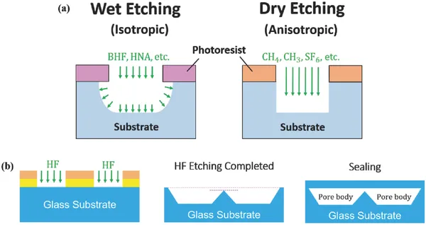
The MSAP process, or Modified Semi-Additive Process, represents a critical advancement in printed circuit board (PCB) manufacturing, enabling the production of high-density interconnects with finer line widths and spacing. This technique builds on traditional subtractive methods by selectively adding copper layers through electroless and electrolytic plating, followed by precise etching. For engineers and designers searching for information on the MSAP process, this tag serves as a comprehensive resource, covering its technical fundamentals, implementation strategies, and real-world benefits in creating compact, reliable electronics. Understanding the MSAP process is essential for addressing modern demands in industries such as consumer electronics, telecommunications, and automotive systems, where miniaturization and signal integrity are paramount. By allowing feature sizes down to 25 microns or smaller, it supports the development of multilayer PCBs that handle high-speed data transmission without compromising performance. Practical applications include smartphones, wearables, and advanced driver-assistance systems (ADAS), where space constraints require innovative fabrication techniques. Key best practices involve optimizing seed layer deposition to ensure uniform plating, selecting appropriate photoresists for fine patterning, and conducting thorough process controls to minimize defects like under-etching or over-plating. Professionals seeking to integrate the MSAP process into their workflows will find value in exploring articles that detail material selections, equipment requirements, and comparative analyses with other methods like full additive or subtractive processes. These insights can guide decisions on scalability, cost efficiency, and yield improvement, ultimately enhancing product reliability. For those troubleshooting common challenges or aiming to innovate in PCB design, the resources grouped under this tag offer in-depth discussions on emerging trends and case studies from leading manufacturers.
Technical Articles
Get in Touch
Send Message
- Products & Service
- Company
- About AIVON
- Contact
- News
- Blog
- Certification
-


- Payment
-


2026 AIVON.COM All Rights Reserved