PCB Bending
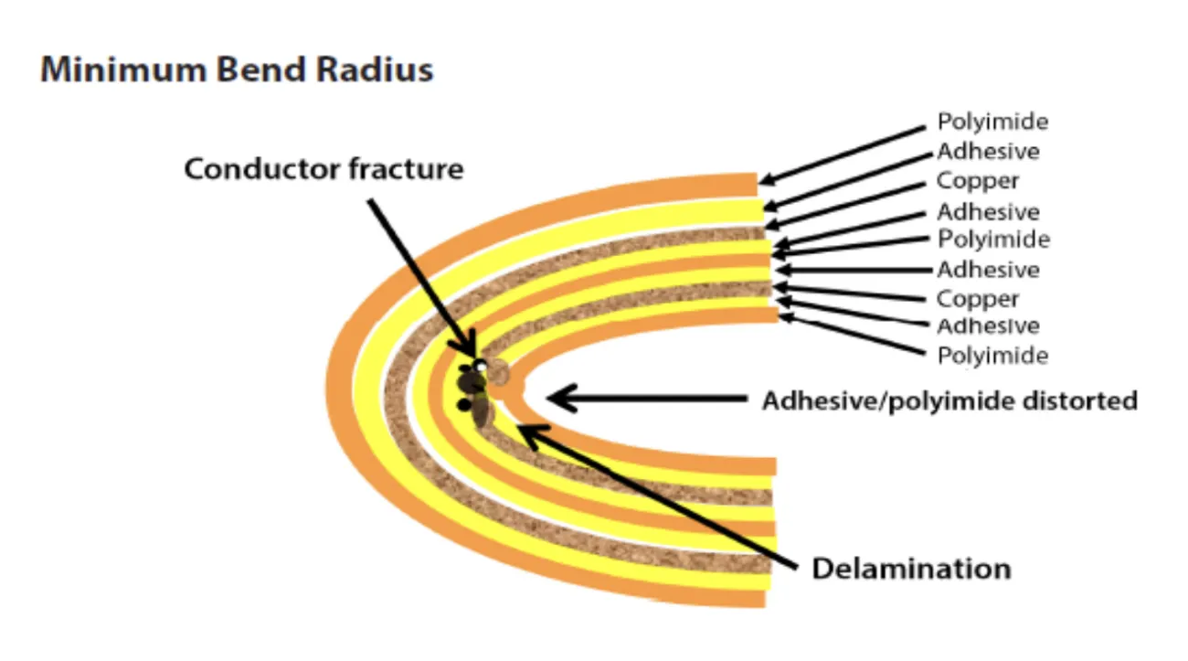
PCB bending refers to the specialized techniques and considerations involved in designing, manufacturing, and assembling printed circuit boards that can flex or curve without compromising functionality. This tag encompasses a range of topics essential for engineers, designers, and hobbyists working on flexible electronics, where traditional rigid PCBs fall short. Whether you are developing wearable devices, automotive sensors, or compact consumer gadgets, understanding PCB bending allows for innovative form factors that adapt to space constraints and dynamic environments. In practice, PCB bending often involves flexible substrates like polyimide films, which enable circuits to withstand repeated flexing. Key applications include medical implants that conform to the body, foldable smartphones, and aerospace components that endure vibration. By exploring the articles under this PCB Bending tag, you can gain actionable insights into material selection, such as choosing the right copper thickness to prevent cracking, and design strategies like incorporating strain relief features to enhance durability. Best practices emphasize thorough testing for bend radius limits and environmental factors, ensuring reliability over time. Common challenges, such as signal integrity issues or delamination, can be mitigated through proper lamination processes and adhesive choices. For those troubleshooting failures or optimizing prototypes, the resources here detail step-by-step guidelines on simulation tools and prototyping methods. Delving into these articles provides practical knowledge to refine your projects, from initial concept to production scaling, helping you achieve robust, flexible PCB solutions that meet industry standards.
Video Guide
No videos found for this tag.
Technical Articles
Get in Touch
Send Message
- Products & Service
- Company
- About AIVON
- Contact
- News
- Blog
- Certification
-


- Payment
-


2026 AIVON.COM All Rights Reserved