Introduction
Flexible printed circuit boards, or PCBs, open up exciting possibilities for electronic hobbyists who want to build compact, adaptable projects. Unlike rigid boards, these bendable circuits conform to curved surfaces, making them ideal for wearables, drones, and portable gadgets. Creating a DIY flexible PCB at home lets you experiment with custom designs without relying on professional fabrication services. This guide covers everything from selecting flexible PCB materials for hobbyists to the etching process, empowering you to prototype innovative circuits. Whether you are crafting a flexible sensor array or a foldable display driver, homemade flexible PCBs combine creativity with practical electronics. Dive in to learn safe, effective methods tailored for your workbench.
What Are Flexible PCBs and Why Build Them at Home?
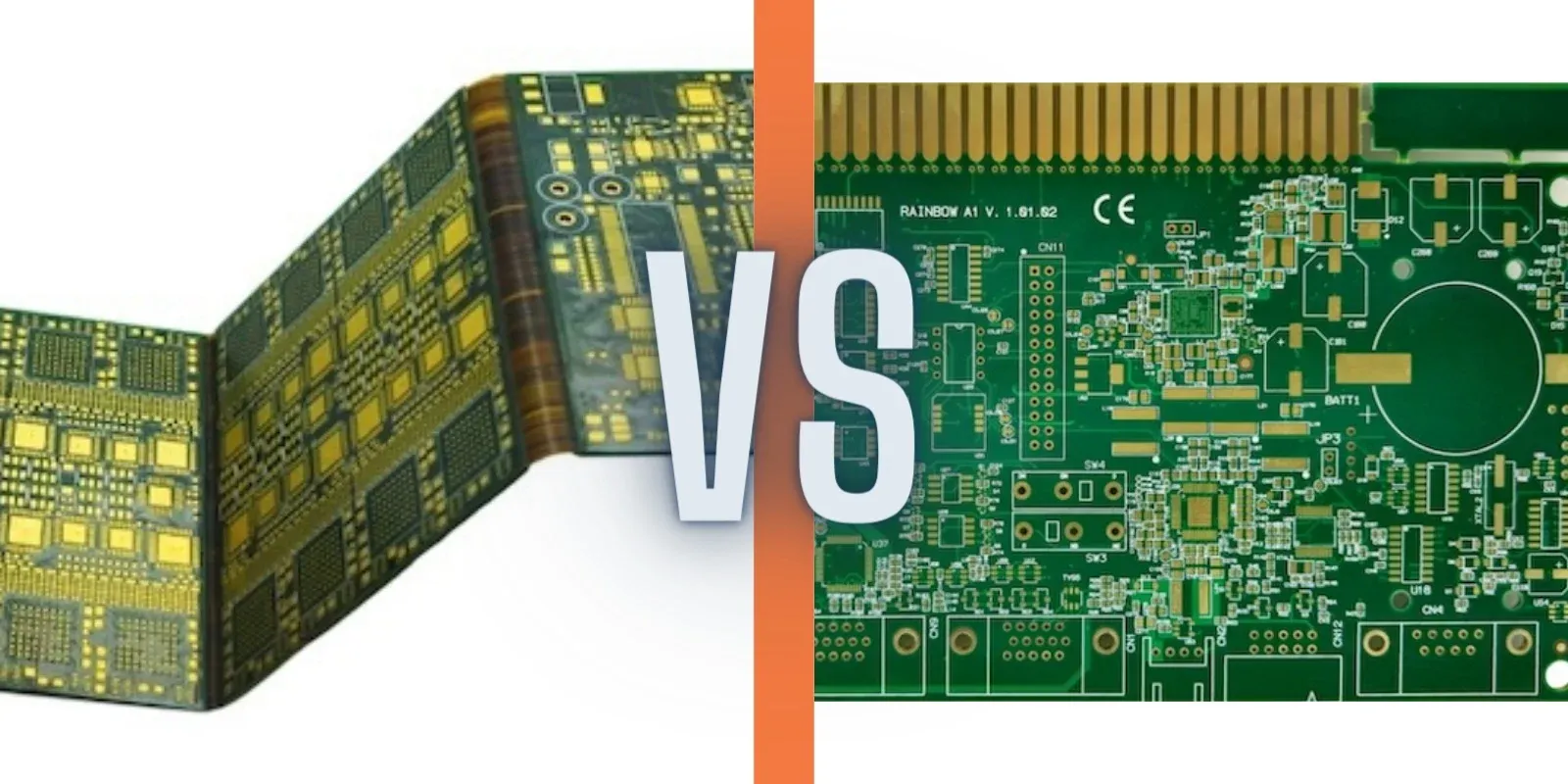
Flexible PCBs consist of conductive traces on a bendable substrate, typically thin polymer films coated with copper foil. These boards maintain electrical performance while enduring repeated flexing, twisting, or folding, which rigid FR4 boards cannot handle. For hobbyists, the appeal lies in their versatility for space-constrained projects like smart clothing or robotic joints. Building a DIY flexible PCB saves costs on small runs and allows rapid iteration during prototyping. You gain hands-on insight into material properties and fabrication limits, fostering deeper understanding of circuit design. Moreover, homemade flexible PCBs encourage experimentation with unconventional form factors that spark unique project ideas.
The core difference from standard PCBs is the substrate material, which prioritizes flexibility over rigidity. Common choices include polyester or polyimide films, both offering good dielectric strength and thermal stability for low-power hobby applications. Why does this matter for home builders? Professional flex boards often exceed hobby budgets, but DIY methods use accessible supplies to achieve similar results. This approach aligns with the maker ethos of self-reliance and customization. Ultimately, mastering DIY flexible PCB creation equips you to tackle advanced electronics challenges.
Key Materials for Homemade Flexible PCBs
Selecting the right flexible PCB materials for hobbyists is crucial for success and safety. Start with a thin copper-clad polyimide or polyester film, available in single-sided sheets around 1 mil thick for optimal bend radius. These substrates provide the necessary tensile strength and insulation without cracking under stress. Photoresist film or dry film serves as the patterning layer, while ferric chloride acts as the etchant for copper removal. Additional supplies include developer solution, protective gloves, and ventilation equipment to handle chemicals responsibly. Always source materials rated for electronics use to ensure reliable conductivity post-etching.
Polyimide stands out for its high-temperature tolerance, up to 200 degrees Celsius in some grades, making it suitable for soldering delicate traces. Polyester offers a cheaper alternative for low-heat projects but has lower moisture resistance. Copper foil thickness, typically 1 oz per square foot, balances flexibility with current-carrying capacity for hobby circuits under 1 amp. Adhesiveless laminates prevent delamination during bends, a common failure mode. Test small samples first to verify adhesion and flex life. These choices form the foundation of a durable homemade flexible PCB.
Safety cannot be overstated when handling etchants and films. Wear nitrile gloves, eye protection, and work in a well-ventilated area to avoid fumes. Dispose of waste per local regulations to protect the environment. Store materials in dry conditions to prevent oxidation or hydrolysis. With proper preparation, your material kit supports multiple prototypes. This setup keeps costs under 50 dollars for several boards.
Technical Principles Behind Flexible PCB Design and Fabrication
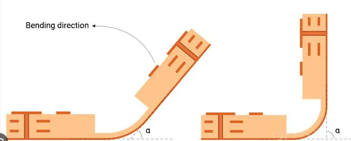
The engineering of flexible PCBs relies on matching substrate properties to mechanical stresses. Bending introduces tensile strain on the outer layer and compression on the inner, so trace widths must exceed minimums to avoid cracking, often 0.2 mm for hobby tools. Copper ductility allows it to elongate without fracturing, but sharp bends reduce cycle life. Design rules emphasize gradual curves with radii at least four times the board thickness. Coverlays, thin insulating films, protect traces from abrasion and environmental factors. Understanding these principles ensures your DIY flexible PCB withstands real-world use.
Adhesion between copper and substrate follows IPC standards for flexible circuits, such as IPC-6013, which specifies peel strength tests. These guidelines verify that laminates endure 180-degree peels without separation. Thermal expansion mismatch can cause warping during soldering, so select materials with similar coefficients. Flex life depends on dynamic bending radius; tighter radii accelerate fatigue. Static folds, common in wearables, tolerate smaller radii. Incorporate strain relief vias or anchors to distribute stress evenly across traces.
Etching chemistry plays a pivotal role in pattern definition. Ferric chloride selectively dissolves exposed copper via redox reaction, leaving insulated paths intact. Uniform etchant temperature, around 40 degrees Celsius, prevents undercutting that widens traces undesirably. Agitation ensures even attack rates, critical for fine-pitch designs under 0.5 mm. Post-etch cleaning removes residues to avoid shorts. These mechanisms translate design files into functional bendable circuits.
Step-by-Step Guide to DIY Flexible PCB Etching
Begin your flexible PCB etching process by preparing the workspace with trays, timers, and safety gear. Print your design mirror-imaged on glossy paper using a laser printer for toner transfer. Laminate the copper-clad film with photoresist by applying heat and pressure via a household iron at low settings. Expose the resist under UV light through a transparency mask for 5 to 10 minutes, depending on light intensity. Develop in sodium carbonate solution to reveal the pattern, then rinse thoroughly. This toner or photo method suits hobbyists without darkroom access.
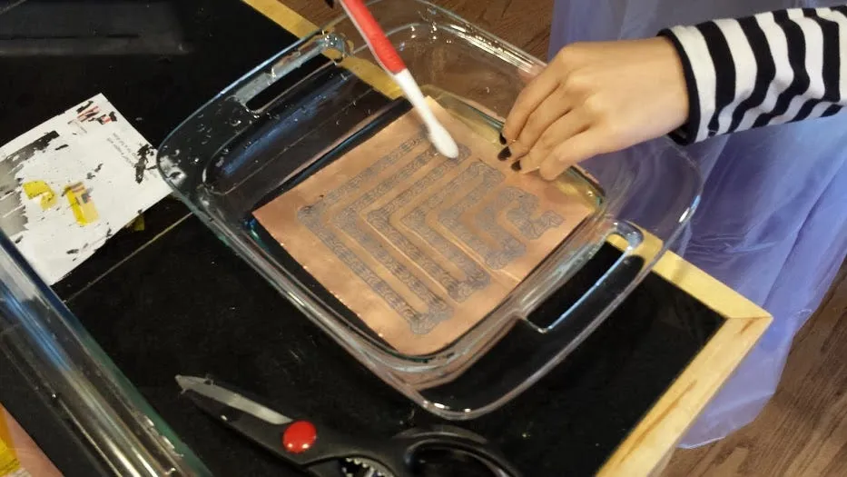
Next, immerse the panel in ferric chloride etchant, agitating gently for 10 to 20 minutes until copper clears. Monitor progress visually to halt over-etching, which thins traces. Neutralize with baking soda solution, strip resist with acetone, and clean with isopropyl alcohol. Inspect under magnification for defects like bridges or pits. Solder components using low-temperature paste to minimize heat damage. Your homemade flexible PCB is now ready for testing and flexing.
For multi-layer attempts, align and bond additional sheets with acrylic adhesive, but single-layer suffices most hobby needs. Practice on scrap to refine timing. Document each step for repeatability.
Best Practices and Troubleshooting for Reliable Results
Adhere to best practices to maximize DIY flexible PCB longevity. Maintain trace spacing at least 0.3 mm to prevent shorts during bends. Apply coverlay or conformal coating post-etching for moisture protection. Test flex cycles by repeatedly bending over a cylinder, aiming for thousands without failure. Bake boards at 100 degrees Celsius for an hour to drive off moisture before soldering, per JEDEC handling guidelines. Store in anti-static bags to avoid ESD damage.
Common issues include resist lifting from poor lamination, solved by even pressure and clean surfaces. Uneven etching stems from stagnant solution; use a bubbler or rocker tray. Warping occurs from asymmetric copper distribution; balance ground planes. If traces crack on flex, widen them or increase bend radius. Solder joint failures link to flux residue; clean meticulously. These fixes elevate hobby prototypes to professional quality.
Incorporate IPC-A-600 acceptability criteria for visual inspection, checking for voids or discoloration. This standard ensures cosmetic and functional integrity without advanced tools. Route signals away from high-stress zones. For power traces, serpentine patterns distribute strain. These strategies prevent field failures in dynamic applications.
Hobbyist Applications and Real-World Insights
DIY flexible PCBs shine in flexible PCB application areas like wearables such as fitness trackers, where circuits wrap around wrists comfortably. In drones, they route signals through folding arms for compact storage. Robotic grippers benefit from conformable sensors on curved surfaces. Hobbyists craft LED matrices that bend into shapes for art installations. These uses demonstrate the freedom of homemade flexible PCBs beyond rigid constraints. Experiment with sensors or actuators to push boundaries.
Troubleshooting a wearable prototype might reveal delamination from sweat exposure; reinforce with silicone sealant. In a drone, vibration shortens flex life, so add damping pads. These insights refine future designs. Share builds in communities for feedback.
Conclusion
Crafting DIY flexible PCBs empowers hobbyists to innovate with bendable circuits tailored to unique projects. From material selection to etching, each step builds skills in flexible PCB fabrication. Prioritize safety, standards compliance, and iterative testing for robust results. Whether prototyping wearables or robotics, these techniques unlock creative potential. Start small, scale up, and enjoy the flexibility of homegrown electronics.
FAQs
Q1: What materials are best for DIY flexible PCB projects?
A1: Flexible PCB materials for hobbyists include polyimide or polyester films clad with 1 oz copper foil. These provide bendability and solderability for low-power circuits. Pair with photoresist for patterning and ferric chloride for etching. Ensure good adhesion to avoid peeling during flex tests. This combination keeps costs low and performance high for homemade flexible PCBs.
Q2: How do I etch a homemade flexible PCB safely at home?
A2: Flexible PCB etching involves UV exposure, development, and immersion in etchant with agitation. Work in a ventilated space wearing gloves and goggles to handle chemicals. Time the etch precisely to prevent over-removal of copper. Rinse and neutralize thoroughly afterward. This process yields precise traces for DIY flexible PCB prototypes.
Q3: What causes failures in DIY flexible PCBs during bending?
A3: Cracks or delamination in DIY flexible PCBs often result from tight bend radii or poor copper adhesion. Use traces wider than 0.2 mm and radii four times board thickness. Balance copper distribution to minimize stress. Test iteratively to identify weak points early. Proper design extends flex life significantly.
Q4: Can beginners make a DIY flexible PCB without special equipment?
A4: Yes, beginners can create homemade flexible PCBs using a laser printer, iron, UV lamp, and household trays. Toner transfer simplifies patterning for single-layer boards. Follow safety protocols for etching. Start with simple circuits to build confidence. Results rival basic professional flex boards.
References
IPC-6013D — Qualification and Performance Specification for Flexible and Rigid-Flex Printed Boards. IPC, 2014
IPC-A-600K — Acceptability of Printed Boards. IPC, 2020
JEDEC J-STD-020E — Moisture/Reflow Sensitivity Classification of Nonhermetic Solid State Surface Mount Devices. JEDEC, 2014