 02:26
02:26
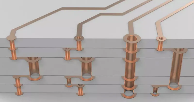
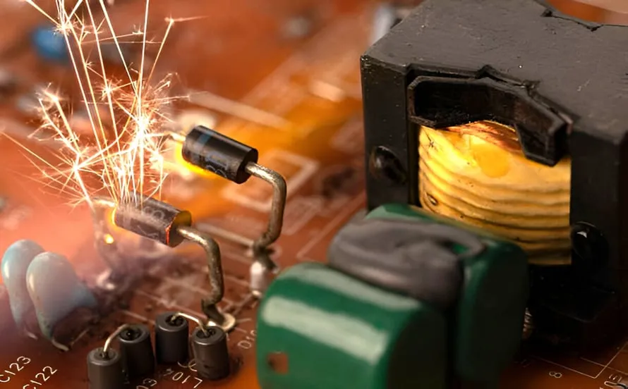
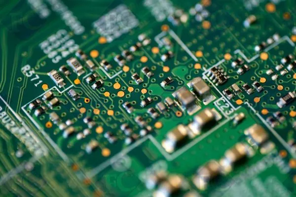
PCB Failure Analysis
PCB Failure Analysis is a critical discipline in electronics engineering, focusing on identifying the root causes of printed circuit board malfunctions to enhance reliability and performance. Whether you are a design engineer troubleshooting a prototype, a quality assurance specialist investigating production defects, or a hobbyist dealing with unexpected breakdowns, understanding failure mechanisms can save time, reduce costs, and prevent recurring issues. This tag compiles expert resources that delve into various aspects of PCB failures, from thermal stress and solder joint degradation to electrical overstress and contamination problems. In these articles, you will find practical guidance on conducting thorough analyses using tools like X-ray imaging, thermal cycling tests, and failure mode effects analysis (FMEA). For instance, learn how to pinpoint delamination in multilayer boards or address via failures in high-density interconnects through real-world case studies. We emphasize best practices such as implementing robust design rules, selecting appropriate materials, and performing preventive inspections to mitigate risks early in the development cycle. By applying these insights, professionals can optimize PCB layouts for harsh environments, while manufacturers can improve yield rates and comply with industry standards like IPC-6012. Browsing the content under this tag offers valuable takeaways for refining your approach to diagnostics and remediation. Articles cover emerging trends, such as analyzing failures in flexible PCBs or those induced by environmental factors, providing actionable steps to integrate into your workflow. This collection serves as a go-to reference for building resilient electronics, helping you turn potential setbacks into opportunities for innovation and efficiency.
Video Guide
-
02:26
Technical Articles
Get in Touch
Send Message
- Products & Service
- Company
- About AIVON
- Contact
- News
- Blog
- Certification
-


- Payment
-


2026 AIVON.COM All Rights Reserved