Introduction
Printed circuit boards (PCBs) form the backbone of modern electronics, where reliability directly impacts system performance and safety. PCB burn-in testing serves as a critical process to identify potential weaknesses before deployment in real-world applications. This stress testing PCB method simulates accelerated aging under controlled extreme conditions, weeding out early-life failures that could lead to field issues. Electrical engineers rely on such reliability testing to validate designs against environmental stresses and ensure long-term operational integrity. By subjecting PCBs to thermal, electrical, and sometimes mechanical loads, burn-in testing accelerates failure mechanisms that would otherwise manifest over years of use. Understanding this process empowers engineers to make informed decisions during quality control phases.
What Is PCB Burn-In Testing?
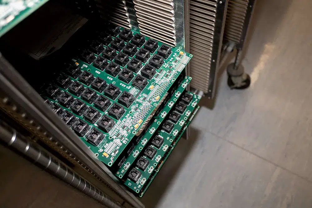
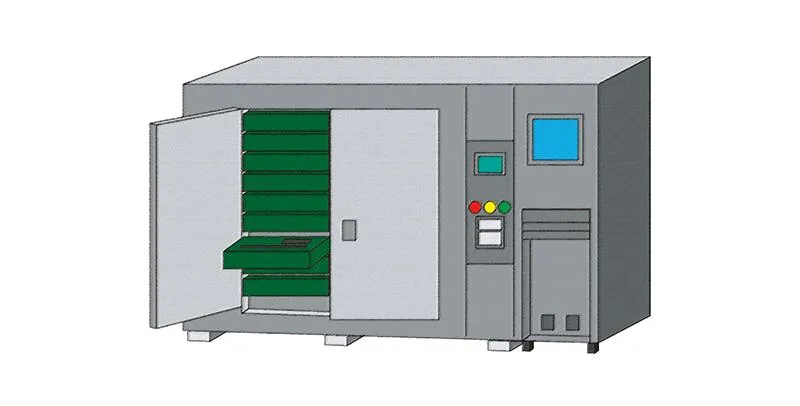
PCB burn-in testing involves operating fully assembled or populated boards at elevated temperatures and voltages beyond normal specifications for a defined duration. This technique, part of broader reliability testing protocols, aims to precipitate infant mortality failures in components or interconnections. Unlike functional testing, which verifies basic operation, burn-in focuses on long-term degradation under stress. Engineers typically conduct it post-assembly to screen for latent defects in solder joints, traces, or passives. The process follows principles of accelerated aging, where time-temperature relationships predict field life. Standards like IPC-6012E outline qualification requirements that incorporate such environmental testing to meet performance criteria.
In practice, burn-in chambers maintain steady high temperatures, often between operating limits and material glass transition points, while power is applied to active circuits. Duration varies based on application criticality, ranging from hours to weeks, with monitoring for parametric drifts or outright failures. This method distinguishes itself from highly accelerated stress tests by emphasizing steady-state stress rather than rapid cycling. Electrical engineers appreciate its role in quantifying mean time between failures (MTBF) estimates without fabricating extrapolated data. Post-test analysis reveals failure modes, guiding design iterations.
Table: PCB Burn-In Testing vs. Other Common Reliability Tests
| Test Type | Primary Stress | Purpose | Typical Duration |
|---|---|---|---|
| PCB Burn-In Testing | Steady high temperature + bias | Screen infant mortality | 24–168 hours |
| Thermal Cycling / HALT | Rapid temperature swings | Identify wear-out mechanisms | Hundreds to thousands of cycles |
| ESS (Environmental Stress Screening) | Combined thermal, vibration, power cycling | Precipitate manufacturing defects | Variable, shorter |
| Functional Testing | Normal operating conditions | Verify basic performance | Minutes to hours |
Why It Matters: The Role in Long-Term Reliability
Early detection of defects through PCB burn-in testing prevents costly recalls and enhances customer trust in high-reliability sectors like aerospace and medical devices. Without stress testing PCB assemblies, random early failures can undermine system uptime, leading to cascading issues in interconnected electronics. Reliability testing bridges the gap between manufacturing variability and field demands, aligning with factory quality control objectives. Engineers use it to validate material choices and process controls against real-world stressors like thermal expansion mismatches. In competitive markets, proven reliability differentiates products, reducing warranty claims and extending service life. This aligns with broader PCB quality control and testing procedures used across production.
Accelerated aging during burn-in mimics cumulative damage from power-on hours, humidity exposure, and voltage transients. This proactive approach supports compliance with industry benchmarks, ensuring PCBs withstand operational envelopes. For instance, assemblies failing burn-in often reveal issues resolvable pre-shipment, saving downstream PCB failure analysis efforts. Factory insights emphasize integrating burn-in into production flows for consistent outcomes. Ultimately, it fortifies the supply chain against variability in components and fabrication.
The Bathtub Curve and Infant Mortality Failures
The bathtub curve provides the foundational model for understanding why PCB burn-in testing is essential. In the early “infant mortality” phase, failure rates are high due to latent manufacturing defects such as voids in plating, contaminated solder joints, weak dielectric materials, or marginal component quality. These defects cause failures that decrease over time as the weakest units are removed from the population.
Research shows that without screening, these early failures can account for the majority of warranty claims and field returns in the first year. Burn-in testing effectively truncates this high-failure region by forcing marginal devices to fail in the factory. Once boards pass, the remaining population exhibits the low, stable failure rate characteristic of useful life.
Technical Principles Behind PCB Burn-In Testing
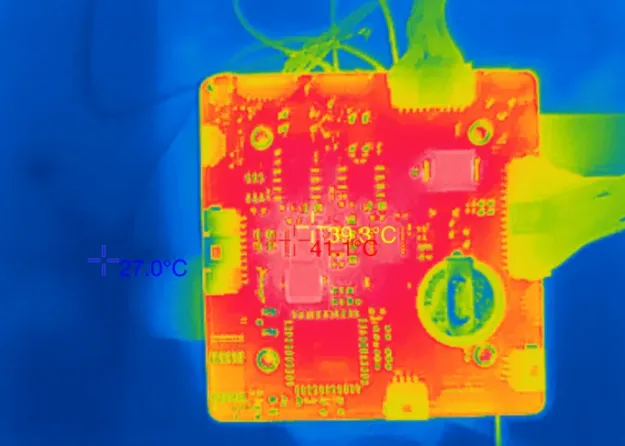
The core principle of PCB burn-in testing relies on accelerating failure mechanisms via the Arrhenius equation, where higher temperatures exponentially speed reaction rates in materials. Electrical migration, delamination, and electromigration intensify under combined thermal-electrical stress, surfacing defects like voids in solder or cracked vias. Stress testing PCB exploits these physics to compress years of aging into days, allowing statistical failure prediction. Engineers monitor key parameters such as leakage current, insulation resistance, and capacitance shifts to detect onset of degradation. Material interactions, including coefficient of thermal expansion (CTE) mismatches between layers, drive many failures observed.
Environmental testing within burn-in incorporates controlled humidity or vibration to replicate service conditions, enhancing comprehensiveness. JEDEC standards guide component-level stresses that propagate to board-level effects during such tests. Factory-driven protocols ensure repeatability, with fixtures distributing uniform power and heat. Data logging captures transients, correlating failures to root causes like trace cracking from fatigue. This structured approach yields actionable insights for refining stackups and layouts.
Common Methods in Stress Testing PCBs
Static burn-in applies constant high voltage and temperature without cycling, ideal for screening passive defects in power supplies. Dynamic burn-in, conversely, cycles power on-off or modulates loads to stress active components like ICs and capacitors. Engineers select methods based on application; for example, high-power boards benefit from dynamic protocols to simulate real workloads. Combined environmental testing adds vibration or humidity per test plans, broadening failure mode coverage. Each method requires calibrated chambers to maintain precision, avoiding overstress that masks true weaknesses.
Thermal profiling ensures even heat distribution across multi-layer boards, mitigating warpage risks. Electrical setups use bed-of-nails fixtures for parallel testing, applying bias voltages scaled to ratings. Duration and thresholds derive from historical data and modeling, not arbitrary values. Post-burn-in, functional re-verification confirms survivors. These methods collectively form a robust reliability testing suite.
PCB Burn-In Test Temperatures, Durations, and Industry Standards
Temperature selection balances acceleration against risk of over-stressing good boards. Common ranges:
Industry-Specific Burn-In Parameters Table
| Industry | Typical Temperature | Typical Duration | Key Standards | Primary Defects Targeted |
|---|---|---|---|---|
| Consumer Electronics | 90–125°C | 8–48 hours | IPC-9701, JEDEC JESD22-A108 | Solder joints, capacitors, micro-cracks |
| Industrial Equipment | 100–135°C | 24–48 hours | IPC-6012, MIL-STD-883 | Thermal fatigue, insulation degradation |
| Automotive | 125–150°C (up to 175°C) | 48–120+ hours | AEC-Q100, JEDEC | Electromigration, delamination under vibration/heat |
| Aerospace / Defense / Medical | 125–150°C+ | 48–168 hours | MIL-STD-883 Method 1015, JESD22-A108 | All latent defects; highest safety margin |
Note: Duration is often calculated using Arrhenius-based acceleration factors to achieve equivalent field life targets (e.g., 1,000–10,000 hours of simulated use). Chambers must maintain uniformity within tight tolerances (± a few °C).
Key standards include:
- JEDEC JESD22-A108: Temperature, Bias, and Operating Life – the primary reference for burn-in methodology.
- MIL-STD-883: Method 1015 (Burn-in Test) and related procedures for high-reliability microelectronics.
- IPC-9701 / IPC-6012: Performance test methods and qualification for rigid printed boards.
- AEC-Q100: Automotive-grade stress testing.
These standards ensure repeatability, safety, and comparability of results.
Best Practices for Effective PCB Burn-In Testing
Establish clear acceptance criteria upfront, defining pass-fail based on parametric limits and visual inspections. Select burn-in conditions conservatively, typically 1.5 to 2 times nominal ratings, to avoid irrelevant failures. Factory protocols should include pre-burn-in electrical characterization for delta comparisons. Use dedicated fixtures with thermal pads for uniform contact, reducing hotspots. Monitor chamber uniformity and log data continuously for traceability. Integrate with overall quality systems like ISO 9001:2015 to document processes systematically.
Sample sizes matter; test representative lots covering process variations. Collaborate with design teams to incorporate test points early. After failures, perform immediate PCB failure analysis using cross-sectioning or X-ray to inform corrections. Scale testing economically, starting with 100% for prototypes and sampling for volume. Regular equipment calibration upholds standard-aligned results. These practices ensure stress testing PCB delivers maximum value.
Integrating PCB Failure Analysis After Burn-In
Failures from burn-in often manifest as opens, shorts, or parametric drifts, traced via systematic PCB failure analysis. Visual microscopy identifies surface cracks, while dye-and-penetrant reveals hidden voids. Cross-sectional analysis exposes inter-layer delaminations from moisture ingress. Electrical fault isolation pinpoints hot carriers or migration paths. Engineers correlate findings to stress conditions, refining future tests.
Non-destructive techniques like acoustic microscopy detect subsurface flaws efficiently. Dye testing highlights microcracks in vias. Thermal analysis post-failure reconstructs heat profiles. Documentation feeds failure mode effects analysis (FMEA), preventing recurrences. This closed-loop approach elevates reliability testing efficacy. For a deeper look at techniques such as cross-sectional analysis and root-cause identification, see our guide to rigid PCB failure analysis.
Applications in High-Reliability Industries
Aerospace and Defense: Long-duration missions demand near-zero early failures. Burn-in at 125–150°C for 100+ hours per MIL-STD-883 weeds out latent defects in avionics, satellites, and radar systems.
Medical Devices: Patient safety is paramount. Implantable and life-support equipment uses stringent burn-in protocols combined with failure analysis to ensure reliability under body temperatures and electrical loads.
Automotive: ADAS, EV powertrains, and engine controls face extreme thermal cycling and vibration. AEC-Q100-qualified burn-in at elevated temperatures simulates decades of driving in days.
Industrial and Telecom: Servers, robotics, and infrastructure equipment benefit from reduced downtime. Dynamic burn-in helps ensure 24/7 operational stability.
In all cases, PCB burn-in testing translates directly into higher MTBF, lower warranty costs, and stronger brand reputation.
Conclusion
PCB burn-in testing stands as an indispensable tool for ensuring long-term reliability through deliberate stress application. By accelerating aging and exposing weaknesses, it safeguards against early failures in demanding applications. Electrical engineers benefit from its factory-aligned insights, standard-referenced protocols, and integration with failure analysis. Adopting best practices maximizes its impact, from test planning to post-analysis actions. Ultimately, consistent implementation fortifies PCB integrity across the product lifecycle, aligning with quality imperatives.
FAQs
Q1: What distinguishes PCB burn-in testing from other reliability testing methods?
A1: PCB burn-in testing focuses on steady-state elevated temperature and voltage to screen infant mortality, unlike thermal cycling which emphasizes expansion-contraction fatigue. It accelerates aging specifically for early defect precipitation, complementing environmental testing like HAST. Engineers use it post-assembly for assembled board validation, ensuring stress testing PCB targets operational weaknesses effectively. This method provides high confidence in long-term performance without excessive cycling wear.
Q2: How does accelerated aging in PCB burn-in testing predict field life?
A2: Accelerated aging applies physics-based models to equate lab stress to field equivalents, revealing degradation rates in materials and joints. Monitoring shifts in resistance or capacitance during tests informs reliability projections. Factory protocols standardize conditions for repeatable outcomes in stress testing PCB. It directly supports decisions on warranty periods and redesigns, grounded in observed failure distributions.
Q3: What role does environmental testing play in PCB burn-in protocols?
A3: Environmental testing enhances PCB burn-in by adding humidity, vibration, or pressure to simulate combined field stresses. This uncovers interactions like corrosion-electromigration absent in pure thermal burn-in. Standards guide severity levels for comprehensive reliability testing. Engineers analyze failures to optimize coatings or layouts, preventing real-world issues.
Q4: Why is PCB failure analysis essential after burn-in testing?
A4: PCB failure analysis dissects burn-in rejects to identify root causes like via cracks or solder fatigue, informing process tweaks. Techniques from microscopy to fault isolation provide data for FMEA updates. It closes the reliability testing loop, reducing future defect rates. Factory insights ensure scalable improvements across production.
References
IPC-6012E — Qualification and Performance Specification for Rigid Printed Boards. IPC, 2017
JEDEC J-STD-020E — Moisture/Reflow Sensitivity Classification. JEDEC, 2014
ISO 9001:2015 — Quality Management Systems. ISO, 2015


