Introduction
Rigid printed circuit boards form the backbone of most electronic assemblies, supporting components under demanding operational conditions. Failures in these boards can lead to system downtime, costly rework, and safety risks in applications from consumer devices to aerospace systems. Rigid PCB failure analysis techniques play a crucial role in dissecting these issues, revealing hidden defects that compromise performance. By systematically identifying rigid PCB failure modes, engineers can trace problems back to design, materials, or manufacturing origins. This process not only resolves immediate concerns but also informs rigid PCB root cause analysis to enhance future reliability. Ultimately, investing in thorough rigid PCB reliability testing prevents recurrence, ensuring long-term product integrity.
In high-stakes industries, where even minor board failures cascade into major disruptions, proactive analysis becomes essential. Electrical engineers often encounter intermittent shorts or opens that evade initial inspections, underscoring the need for advanced diagnostic approaches. Factory-driven insights emphasize aligning analysis with established protocols to maintain quality control. As boards evolve with higher densities and harsher environments, understanding failure mechanisms grows more complex yet vital.
Understanding Rigid PCB Failure Modes and Their Impact
Rigid PCB failure modes encompass a range of electrical, mechanical, and thermal breakdowns that degrade board functionality over time. Common issues include delamination, where layers separate due to adhesive degradation; trace cracking from mechanical stress; and pad lifting, which disrupts solder joints. Warpage distorts the board's planarity, complicating assembly and leading to misalignment. These modes often stem from mismatched coefficients of thermal expansion or contamination during fabrication. Electrical failures like conductive anodic filamentation create unintended paths between conductors, mimicking shorts.
The industry relevance of recognizing these modes lies in their predictability through patterns observed in production. For instance, moisture ingress accelerates hydrolysis in laminates, promoting delamination under thermal cycling. Engineers must differentiate between early-life failures from process defects and wear-out mechanisms from operational stress. IPC-6012E outlines qualification criteria that help benchmark acceptable performance limits for rigid boards. Addressing these modes early reduces scrap rates and extends field life.
Warpage, often exceeding allowable tolerances, affects high-layer-count boards most severely. It arises from asymmetric curing or copper imbalance during lamination. Such deformations stress vias and surface mounts, accelerating fatigue. Reliability suffers as warped boards exhibit higher rejection rates in automated assembly lines. Quantifying these impacts through data logging aids in prioritizing analysis efforts.
Key Mechanisms Behind Rigid PCB Failures
Several engineering mechanisms drive rigid PCB failure modes, rooted in material interactions and process variables. Thermal mismatch between copper foil and substrate generates stresses during soldering or operation, leading to microcracks in vias. Moisture absorption, if not controlled, forms steam pockets under heat, causing pops or delamination. Contaminants like flux residues promote electrochemical migration, forming dendritic growths between traces.
Manufacturing-induced defects, such as drill smear or plating voids, evolve into opens under vibration. Poor glass transition temperature alignment in multilayers exacerbates warpage during reflow. These mechanisms interact; for example, a plated-through hole with inadequate barrel support fails under thermal shock. Understanding these interactions requires layered investigation beyond surface symptoms.
Vibration and mechanical shock propagate fatigue in solder joints and inner traces, common in automotive or industrial uses. Cyclic loading widens preexisting defects from drilling or etching. Reliability testing simulates these conditions to expose weak points. Factory insights stress controlling drill parameters and etch rates to minimize initial flaws.
Rigid PCB Failure Analysis Techniques
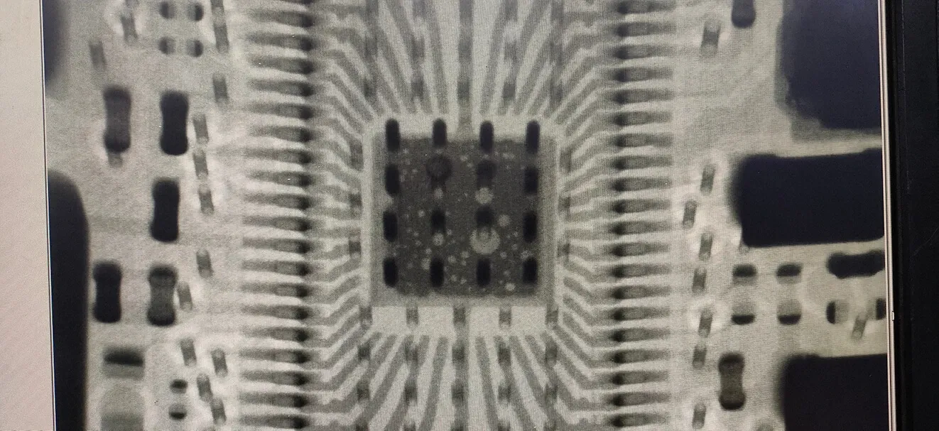
Rigid PCB failure analysis techniques span non-destructive and destructive methods, selected based on failure symptoms and board value. Visual inspection under stereomicroscopy reveals surface anomalies like discoloration or lifting. X-ray imaging detects internal voids, misaligned drills, or bridging without disassembly. Scanning acoustic microscopy identifies delamination or cracks via ultrasonic waves, ideal for multilayer boards.
Electrical testing, including flying probe or bed-of-nails, maps opens, shorts, and resistance shifts. For intermittent faults, environmental stressing like temperature cycling provokes failures. Dye and penetrant tests highlight cracks by capillary action, followed by baking to reveal paths. These techniques provide data for rigid PCB root cause analysis.
Destructive cross-sectioning polishes samples to expose microstructures, analyzed via SEM for fracture origins. Fourier transform infrared spectroscopy detects contaminants or resin degradation. Combining techniques, such as electrical fault isolation with thermal imaging, pinpoints hotspots. Engineers sequence methods from least to most invasive to preserve evidence.
Sampling strategies ensure representativeness, avoiding bias from outliers. Documentation throughout maintains chain of custody for reports. These protocols align with quality control standards, enhancing traceability.
Rigid PCB Root Cause Analysis: A Step-by-Step Approach
Rigid PCB root cause analysis follows structured methodologies like fault tree analysis or the 5 Whys to dissect failure chains. Begin with failure replication under controlled conditions to confirm symptoms. Gather inputs from design files, process logs, and supplier data. Categorize causes into design, material, process, or usage buckets.
Fishbone diagrams visualize contributors, such as plating chemistry for via failures. Statistical process control charts identify excursions in lamination pressure or bake times. J-STD-020E guides moisture sensitivity assessments, linking humidity to popcorn effects. Validation through designed experiments confirms causal links.
Corrective actions target verified roots, like adjusting cure cycles for warpage. Preventive measures extend to supplier audits and incoming inspections. Iterative reviews refine analysis templates for recurring modes. This systematic approach minimizes false positives and accelerates resolutions.
Suggested Reading: Mastering Rigid PCB Design: A Comprehensive Guide for Beginners
Best Practices for Rigid PCB Reliability Testing and Prevention
Rigid PCB reliability testing employs accelerated life tests to predict field performance. Thermal cycling per IEC standards simulates expansion mismatches, exposing weak interfaces. Highly accelerated stress tests combine temperature, humidity, and bias to induce migration. Mechanical shock and vibration tables replicate handling and operation stresses.
Design for reliability starts with stackup symmetry and material selection per CTE matching. Process controls include bake-out before lamination and plasma cleaning for surfaces. Incoming material verification checks glass fabric weave and resin content uniformity. Post-fabrication, 100% electrical testing catches early defects.
Assembly compatibility demands flatness within specifications to avoid head-in-pillow defects. Feedback loops from field returns refine protocols. Implementing these practices reduces failure rates significantly. Standards like IPC-A-600K define acceptability criteria, guiding inspections. For complementary techniques, see our guide on PCB burn-in testing.
Troubleshooting Common Scenarios
In one scenario, intermittent opens in high-speed traces pointed to CAF after humidity exposure. Cross-sectioning revealed ionic residues from etch processes. Adjusting rinse cycles and adding conformal coating resolved it. Another case involved warpage in thick cores, traced to copper weight imbalance. Symmetric foils and controlled pressing fixed future builds.
Pad cratering during reflow often links to aggressive fluxes or brittle epoxies. Dye testing exposed interface weaknesses. Switching to low-loss materials improved joint strength. These examples highlight how targeted rigid PCB failure analysis techniques yield actionable insights.
Conclusion
Rigid PCB failure analysis remains indispensable for maintaining electronic system reliability amid increasing complexity. By mastering failure modes, analysis techniques, root cause methods, and reliability testing, engineers safeguard product lifecycles. Factory-driven adherence to standards ensures consistent outcomes. Proactive prevention through design and process refinements minimizes risks. Ultimately, these efforts deliver robust boards that withstand real-world demands, fostering trust in electronic designs.
FAQs
Q1: What are the most common rigid PCB failure modes?
A1: Rigid PCB failure modes include delamination, trace cracking, warpage, pad lifting, and conductive anodic filamentation. Delamination arises from moisture or thermal stress degrading adhesives. Trace cracks develop under mechanical or cyclic loading. Warpage distorts planarity from curing imbalances. Identifying these early via inspections prevents assembly issues and field failures.
Q2: How do rigid PCB failure analysis techniques help in root cause identification?
A2: Rigid PCB failure analysis techniques like X-ray, cross-sectioning, and dye penetrant testing isolate defects non-destructively or destructively. Electrical mapping pinpoints opens or shorts. Acoustic microscopy detects subsurface delamination. Combining methods with process data enables rigid PCB root cause analysis. This structured approach verifies causal factors, guiding corrections.
Q3: Why is rigid PCB reliability testing essential for prevention?
A3: Rigid PCB reliability testing, such as thermal cycling and HAST, accelerates failure modes to predict longevity. It exposes weaknesses in materials or processes under stress. Standards define test parameters for consistency. Results inform design tweaks and controls. Regular testing reduces rigid PCB failure modes in production and service.
Q4: What steps follow rigid PCB root cause analysis for prevention?
A4: After rigid PCB root cause analysis, implement corrective actions like process adjustments or material changes. Validate via retesting. Update specifications and train teams. Monitor via SPC for sustained improvements. Preventive audits ensure compliance. This closes the loop, minimizing future rigid PCB failure modes.
References
IPC-6012E — Qualification and Performance Specification for Rigid Printed Boards. IPC, 2017
IPC-A-600K — Acceptability of Printed Boards. IPC, 2020
J-STD-020E — Moisture/Reflow Sensitivity Classification. JEDEC, 2014