PCB Masking
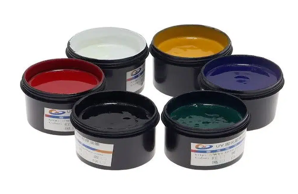
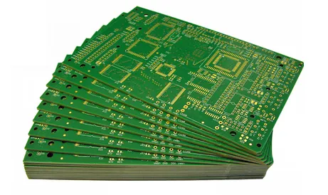
PCB masking plays a critical role in the design and manufacturing of printed circuit boards, serving as a protective layer that shields copper traces from oxidation, prevents solder bridges during assembly, and enhances overall board durability. This tag, PCB Masking, encompasses a range of topics related to solder mask application, materials, and techniques used in electronics production. For engineers, hobbyists, and manufacturers searching for information on this keyword, understanding PCB masking is essential to achieving reliable circuit performance and compliance with industry standards such as IPC-6012. In practical terms, effective PCB masking involves selecting the right type of mask, whether liquid photoimageable, dry film, or epoxy-based, to suit specific project needs like high-density interconnects or harsh environmental conditions. Best practices include ensuring uniform coating thickness to avoid defects like voids or pinholes, which can lead to short circuits or reduced insulation resistance. Users often seek guidance on troubleshooting common issues, such as mask adhesion problems or color variations that affect aesthetic and functional outcomes. By applying these insights, you can optimize your PCB designs for better yield rates and longevity, particularly in applications ranging from consumer electronics to automotive systems. The articles grouped under this tag delve into real-world examples, step-by-step processes for mask application, and comparisons of masking technologies to help you make informed decisions. Whether you are refining a prototype or scaling up production, these resources offer valuable knowledge to address your specific challenges in PCB fabrication.
Video Guide
No videos found for this tag.
Technical Articles
Get in Touch
Send Message
- Products & Service
- Company
- About AIVON
- Contact
- News
- Blog
- Certification
-


- Payment
-


2026 AIVON.COM All Rights Reserved