 00:57
00:57
Solder Mask Defined
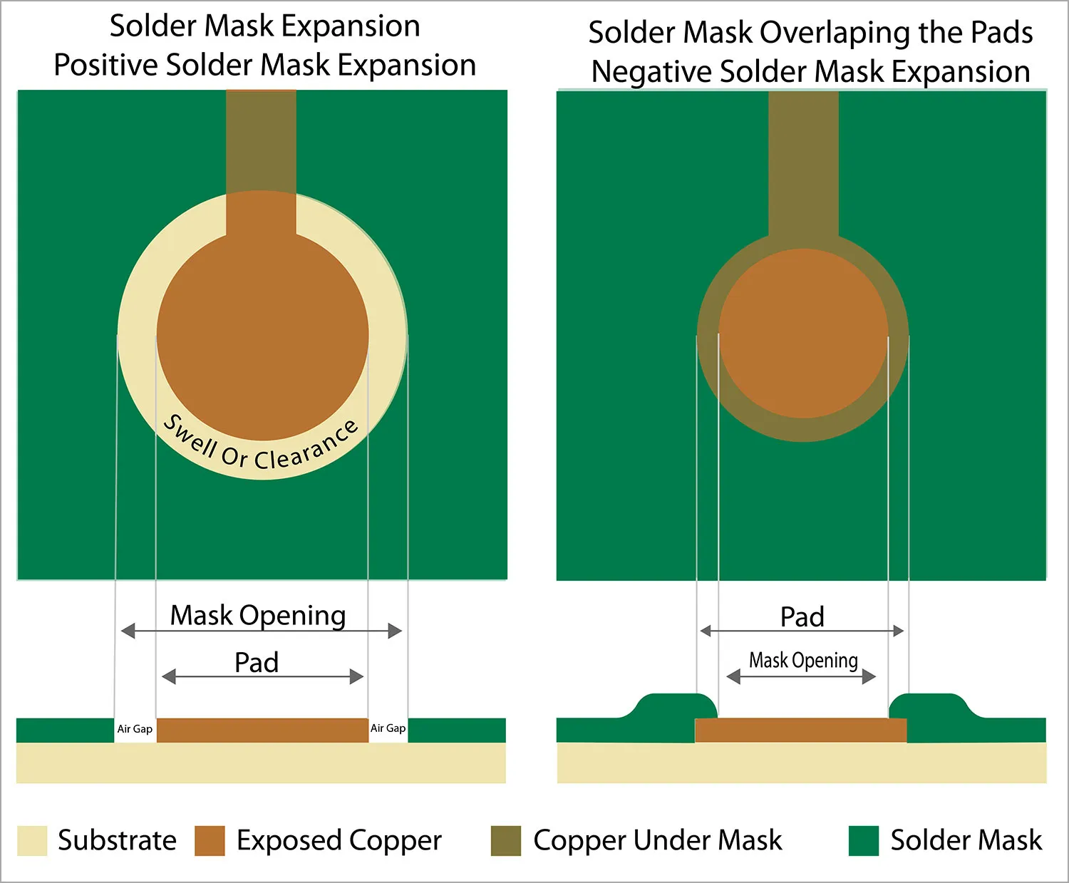
Solder mask defined pads represent a critical technique in printed circuit board (PCB) design, where the solder mask layer overlaps the edges of copper pads to precisely control their exposed area. This approach enhances reliability by preventing solder bridging during assembly and improving adhesion for fine-pitch components. Engineers and designers often search for information on solder mask defined methods to optimize their layouts for high-density applications, such as in consumer electronics, automotive systems, and telecommunications equipment. By defining pads through the solder mask, you can achieve tighter tolerances and reduce the risk of defects like tombstoning or insufficient solder joints, which are common challenges in surface-mount technology (SMT). Understanding the solder mask defined strategy is essential for anyone involved in PCB fabrication or prototyping. It contrasts with non-solder mask defined pads, where the mask clears entirely around the pad, offering different benefits in terms of solderability and mechanical strength. In practice, selecting solder mask defined pads is particularly advantageous for ball grid array (BGA) packages and other advanced components that demand precise alignment and thermal management. Best practices include ensuring a minimum overlap of 0.05mm to 0.1mm to balance protection and solder flow, while also considering the mask's material properties to withstand reflow temperatures. Designers should verify these specifications in their Gerber files to avoid manufacturing issues. For those looking to apply these concepts effectively, our articles under the Solder Mask Defined tag provide detailed case studies and tutorials on integration with CAD software like Altium or KiCad. These resources cover real-world scenarios, from troubleshooting common errors to scaling designs for mass production, helping you refine your PCB projects with confidence.
Video Guide
-
00:57
Technical Articles
Get in Touch
Send Message
- Products & Service
- Company
- About AIVON
- Contact
- News
- Blog
- Certification
-


- Payment
-


2026 AIVON.COM All Rights Reserved