Introduction
Solder mask serves as a vital protective layer on printed circuit boards, shielding copper traces from oxidation and environmental damage during assembly and operation. In surface mount technology processes, the precise management of solder mask around pads directly influences joint reliability and yield rates. Solder mask expansion refers to the intentional enlargement of the mask opening beyond the copper pad boundaries, ensuring proper solder wetting and fillet formation. This parameter, often called solder mask pullback, accommodates manufacturing tolerances like mask registration errors. Engineers must grasp solder mask expansion values to avoid common defects such as bridging, incomplete wetting, or tombstoning. Proper implementation aligns with assembly best practices, enhancing overall PCB performance.
What Is Solder Mask Expansion and Why It Matters
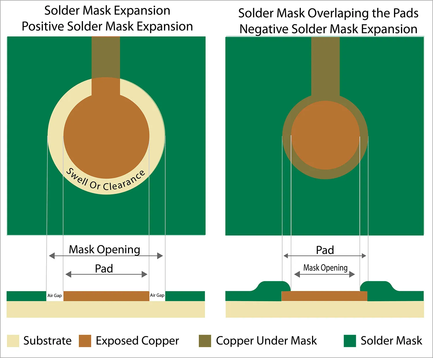
Solder mask expansion defines the clearance distance between the edge of the copper pad and the nearest edge of the solder mask opening. This pullback prevents the mask material from encroaching on the pad surface, which could inhibit solder flow during reflow soldering. In design files, specifying the solder mask opening size larger than the pad creates this expansion uniformly on all sides. Without adequate expansion, solder joints may form with insufficient volume or poor adhesion, leading to early failures under thermal cycling. For electric engineers focused on assembly yields, understanding these dynamics is crucial for troubleshooting intermittent defects in high-volume production.
The relevance intensifies in modern fine-pitch components where pad spacing shrinks below 0.5 mm. Insufficient solder mask expansion values can exacerbate solder beading or bridging between adjacent pads, compromising signal integrity and mechanical strength. Conversely, excessive expansion risks solder wicking onto traces, promoting unintended shorts. Industry standards like IPC-7351 provide guidelines for balancing these factors based on component density and pitch. Mastering solder mask pullback ensures consistent reflow profiles and minimizes rework, directly impacting cost and turnaround times in PCB assembly.
Differentiating Pad Types: Non-Solder Mask Defined vs. Solder Mask Defined Pads
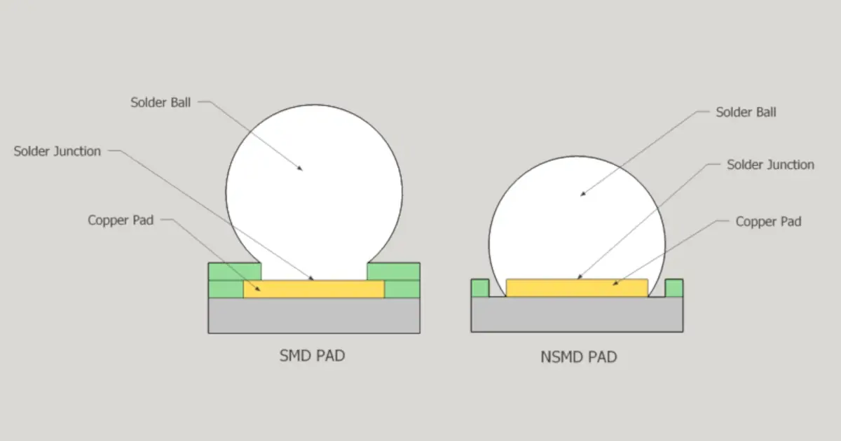
Pads fall into two primary categories: non-solder mask defined (NSMD) and solder mask defined (SMD), each with distinct solder mask interactions. NSMD pads feature a solder mask opening significantly larger than the copper pad, typically with expansion on all sides to expose the full pad for solder wetting. This configuration promotes barrel-shaped joints with optimal volume control, ideal for ball grid arrays and fine-pitch quad flat no-leads. SMD pads, however, have the solder mask opening equal to or smaller than the pad, where the mask edge defines the effective solder joint footprint. Engineers select NSMD for better fatigue resistance in dynamic environments, while SMD suits applications needing precise joint sizing to prevent bridging.
SMD pads solder mask design relies on the mask to constrain solder flow, creating a moat-like barrier around the joint periphery. This approach reduces pad exposure but enhances retention for larger components under vibration. Transitioning between types requires adjusting solder mask opening sizes in layout tools, always verifying against fabricator capabilities. Misapplication, such as using SMD on fine-pitch without sufficient mask web, invites defects like solder extrusion. Practical troubleshooting often reveals NSMD superiority for yields above 99% in high-density boards.
Technical Principles Behind Solder Mask Expansion
Solder mask application involves photolithographic processes where liquid photoimageable (LPI) material coats the board, followed by exposure and development. Registration tolerances, typically 50 to 75 microns, necessitate expansion to guarantee pad exposure despite alignment shifts. Thermal expansion mismatch between mask, copper, and substrate during reflow further justifies pullback, as mask shrinkage could otherwise overlap pads. IPC-SM-840 outlines performance criteria for mask adhesion and thickness, indirectly supporting expansion strategies for reliable insulation between features.
For NSMD pads, expansion facilitates solder fillet formation per IPC-7351 land pattern guidelines, optimizing standoff height and joint geometry. In contrast, SMD configurations demand precise mask edges to control solder standoff, minimizing voiding under components. Engineers calculate opening sizes by adding twice the expansion value to pad diameter, accounting for annular ring integrity. Process variations like panel warp or exposure non-uniformity underscore the need for conservative values in high-reliability assemblies.
Best Practices for Solder Mask Expansion in PCB Design and Assembly
Start by consulting fabricator DFM reports for their specific mask tolerances, then apply solder mask expansion values starting at 75 microns per side for standard pitches above 0.65 mm. For tighter pitches under 0.5 mm, increase to 100 microns to buffer against bridging risks during stencil printing and reflow. Always define expansions explicitly in design rules rather than relying on defaults, ensuring consistency across pad stacks. Verify Gerber previews show clean mask slivers at least 100 microns between openings to prevent webbing failures.
In NSMD designs, pair expansion with solder paste reduction ratios of 90-95% for optimal volume, troubleshooting excess paste-induced defects. For SMD pads solder mask setups, minimize expansion to near zero while maintaining mask overlap for joint definition, ideal for QFNs prone to voiding. Test assemblies with cross-sections to validate fillet heights against J-STD-001 criteria, adjusting iteratively for process windows. Incorporate via-in-pad considerations by extending expansion around exposed vias to avoid solder entrapment.
Collaborate early with assembly partners on stencil thickness, as thinner stencils demand finer expansion tuning to match paste release. Simulate reflow profiles to predict mask behavior under peak temperatures around 260°C, preventing delamination. Document rationale in fab notes, specifying "solder mask pullback per IPC-7351 nominal density" for traceability.
Troubleshooting Common Issues with Solder Mask Expansion
Insufficient solder mask expansion often manifests as de-wetting, where solder beads up away from pad edges due to mask contamination. Inspect under 10x magnification for mask creep, then redesign with 25-micron increments until resolved. Bridging in fine-pitch arrays signals over-expansion or poor registration; counter by tightening paste apertures and validating mask alignment post-lamination.
Tombstoning on passives traces to uneven wetting from asymmetric expansion, fixable by symmetrizing openings and optimizing ramp-up rates. For SMD pads, mask cracking under thermal stress indicates thin application; specify 15-25 micron thickness per IPC-SM-840. Systematic failure analysis via X-ray and dye penetrant reveals root causes, guiding refinements for next-spin yields.
Conclusion
Solder mask expansion remains a cornerstone of robust PCB assembly, balancing exposure for wetting against protection from shorts. By differentiating NSMD and SMD approaches and adhering to standards like IPC-7351, engineers achieve high-reliability joints. Practical implementation involves DFM collaboration, precise Gerber specs, and iterative troubleshooting. Prioritizing solder mask opening size and pullback values minimizes defects, streamlines production, and extends board lifespan. Forward-thinking designs incorporate these practices from layout inception for superior assembly outcomes.
FAQs
Q1: What are typical solder mask expansion values for NSMD pads?
A1: For non-solder mask defined pads, expansion values commonly range from 75 to 125 microns per side, accommodating mask registration tolerances. This ensures full pad exposure for reliable solder fillets during reflow. Adjust based on pitch and fabricator specs, verifying via DFM feedback to prevent bridging. IPC-7351 guidelines support these for nominal density levels in SMT assembly.
Q2: How does solder mask pullback affect SMD pads solder mask design?
A2: Solder mask pullback in SMD pads limits expansion to define joint size precisely, reducing solder volume for controlled standoff. This troubleshooting-focused approach suits larger components but risks poor wetting if tolerances exceed capabilities. Maintain minimal pullback with robust mask webs to avoid extrusion, aligning with assembly process windows for high yields.
Q3: What is the ideal solder mask opening size for fine-pitch components?
A3: Solder mask opening size exceeds pad dimensions by twice the expansion value, typically 100-150 microns total for pitches below 0.4 mm. This prevents mask overlap while ensuring insulation between pads. Practical verification through prototypes confirms compatibility with stencil and reflow, optimizing for defect-free assembly.
Q4: Why choose NSMD over SMD for high-density boards?
A4: NSMD pads with adequate solder mask expansion offer superior joint strength and fatigue resistance due to larger solder volumes. They excel in fine-pitch scenarios by minimizing bridging risks compared to SMD configurations. Troubleshooting data shows higher yields, making NSMD the go-to for demanding electric engineering applications.
References
IPC-7351B — Generic Requirements for Surface Mount Design and Land Pattern Standard. IPC, 2007
IPC-SM-840D — Qualification and Performance of Permanent Solder Mask. IPC, 2014
IPC-A-610H — Acceptability of Electronic Assemblies. IPC, 2020
J-STD-001H — Requirements for Soldered Electrical and Electronic Assemblies. IPC, 2020


