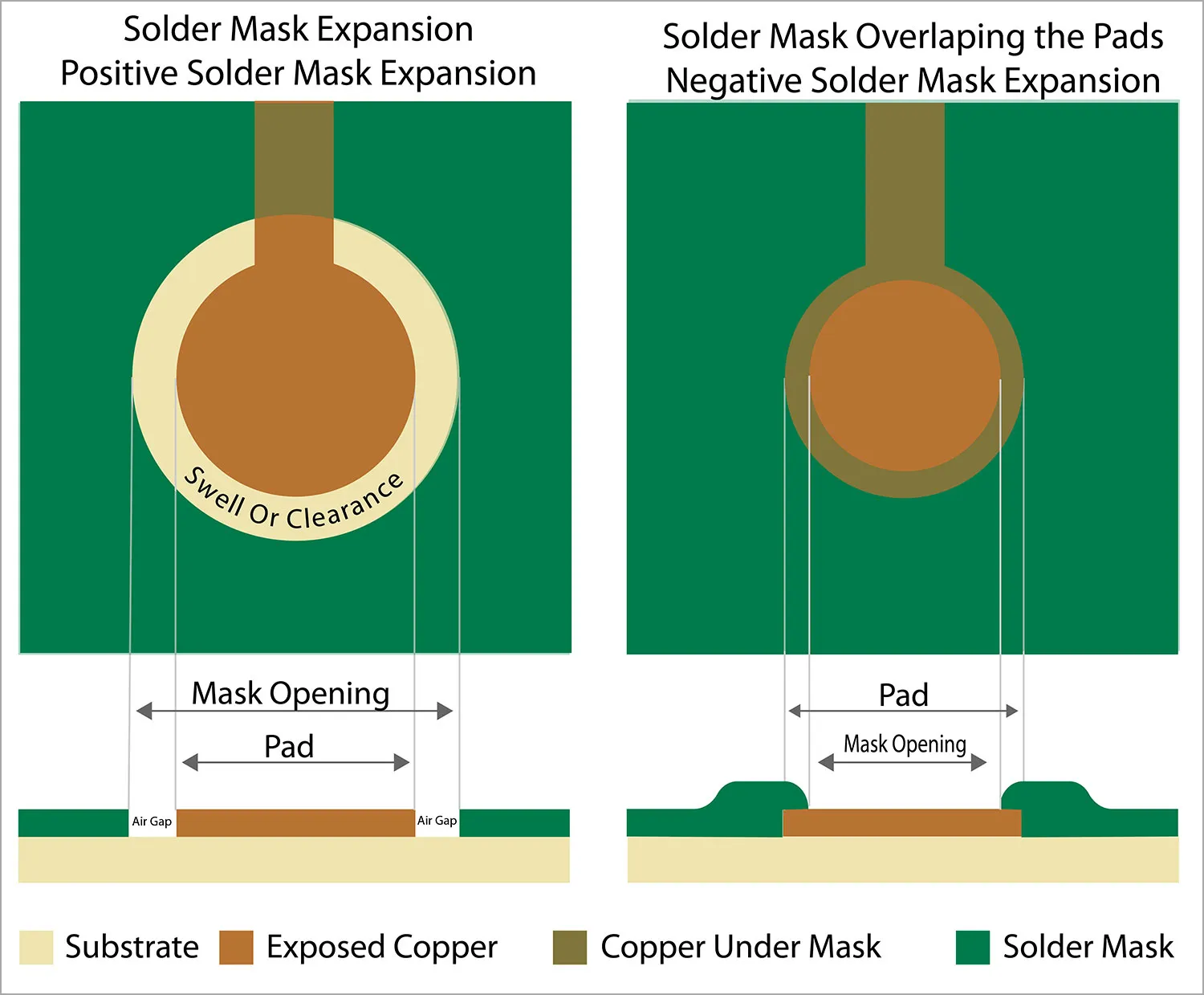
Solder Mask Expansion
Solder mask expansion is a critical aspect of printed circuit board (PCB) design that involves extending the solder mask layer beyond the edges of copper pads and vias. This technique creates a defined clearance, typically measured in mils or millimeters, to prevent solder from bridging between adjacent components during the assembly process. For engineers and hobbyists searching for information on solder mask expansion, understanding this parameter is essential for achieving reliable PCB fabrication and avoiding common manufacturing defects such as shorts or insufficient solder joints. In practice, solder mask expansion helps protect the underlying copper traces from oxidation and environmental damage while ensuring precise solder application. It is particularly useful in high-density designs where components are closely spaced, as it minimizes the risk of mask misalignment that could expose traces or cause tombstoning in surface-mount technology (SMT) assemblies. By optimizing expansion values—often set between 2 to 5 mils depending on the board's complexity and manufacturer guidelines—designers can enhance the overall durability and performance of the PCB. This is especially relevant for applications in consumer electronics, automotive systems, and medical devices, where reliability under thermal stress or vibration is paramount. To implement effective solder mask expansion, consider factors like pad size, via types, and the specific fabrication process. Best practices include consulting IPC standards, such as IPC-7351, for recommended clearances and performing design rule checks (DRC) in software tools like Altium or KiCad. Adjusting expansion based on solder paste requirements can also improve yield rates in production runs. For those delving deeper into PCB layout techniques, the articles linked under this tag offer detailed case studies and tutorials on balancing expansion with other design elements, providing practical guidance to refine your projects.
Video Guide
No videos found for this tag.
Technical Articles
Get in Touch
Send Message
- Products & Service
- Company
- About AIVON
- Contact
- News
- Blog
- Certification
-


- Payment
-


2026 AIVON.COM All Rights Reserved