Stencil Optimization
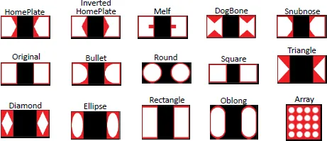
Stencil optimization plays a crucial role in the PCB assembly process, focusing on refining the design and application of solder paste stencils to achieve higher precision and efficiency. For engineers and manufacturers searching for ways to enhance stencil performance, this tag gathers resources that delve into techniques for minimizing defects such as bridging, insufficient paste deposition, or misalignment during surface mount technology (SMT) operations. By optimizing stencil parameters like aperture size, shape, and thickness, users can significantly improve first-pass yields and reduce rework costs in high-volume production environments. Key aspects covered under Stencil Optimization include selecting appropriate stencil materials, such as stainless steel or laser-cut options, and applying best practices for aperture design to match specific component footprints. Practical applications extend to adjusting stencil tension, alignment methods, and cleaning protocols, which are essential for maintaining consistent solder paste transfer across various PCB layouts. These optimizations not only address common challenges in prototyping but also scale effectively for mass production, ensuring reliable electrical connections and overall board integrity. Professionals in electronics design will find actionable insights here, from simulation tools that predict paste release behavior to real-world case studies demonstrating yield improvements. Whether troubleshooting print quality issues or seeking to integrate advanced techniques like nano-coatings for better release properties, the articles linked through this tag offer detailed guidance based on industry standards. Browsing these resources can help refine your assembly processes, leading to more robust and cost-effective PCB manufacturing outcomes.
Video Guide
No videos found for this tag.
Technical Articles
Get in Touch
Send Message
- Products & Service
- Company
- About AIVON
- Contact
- News
- Blog
- Certification
-


- Payment
-


2026 AIVON.COM All Rights Reserved