Via Repair
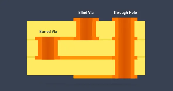
Vias are essential components in printed circuit boards (PCBs), serving as conductive pathways that connect different layers and ensure signal integrity. When vias become damaged due to manufacturing defects, mechanical stress, overheating, or environmental exposure, they can lead to intermittent failures, short circuits, or complete board malfunction. The Via Repair tag on this blog gathers in-depth resources dedicated to diagnosing and fixing these issues, helping electronics professionals, engineers, and hobbyists restore functionality without replacing entire boards. Understanding via repair starts with identifying common problems, such as cracked plating, lifted pads, or contamination. Practical techniques include using specialized tools like via repair kits, which often involve inserting eyelets or applying conductive inks to rebuild the connection. For instance, a step-by-step approach might involve cleaning the damaged area with isopropyl alcohol, drilling out debris if necessary, and then filling the via with epoxy or solder to reestablish conductivity. Best practices emphasize testing for continuity with a multimeter after repairs and applying conformal coatings to prevent future corrosion, ensuring long-term reliability in high-stakes applications like automotive electronics or medical devices. Articles under this tag offer actionable guidance tailored to various skill levels, from basic soldering fixes for prototypes to advanced methods using automated equipment for production runs. By delving into these topics, readers can gain insights into preventive measures, such as designing boards with redundant vias or selecting robust materials during the initial layout phase. Whether you are troubleshooting a one-off repair or optimizing processes in a manufacturing setting, the content here equips you with the knowledge to minimize downtime and extend PCB lifespan. For related discussions on via design or PCB maintenance, browsing connected posts can provide a broader perspective on electronics reliability.
Video Guide
No videos found for this tag.
Technical Articles
Get in Touch
Send Message
- Products & Service
- Company
- About AIVON
- Contact
- News
- Blog
- Certification
-


- Payment
-


2026 AIVON.COM All Rights Reserved