Introduction
In the realm of high-power electronics and industrial applications, thick FR4 PCBs—those exceeding 2.0mm and reaching up to 6.0mm or more—are essential for structural integrity and thermal management. However, moving away from the standard 1.6mm thickness introduces a unique set of manufacturing complexities that often catch designers off guard. At AIVON, our engineering teams frequently encounter data files that do not account for the physical limitations of processing such dense substrates. These oversights result in Engineering Queries (EQs), which pause the production clock and require detailed technical clarifications. Understanding why these queries occur is the first step toward a more efficient and reliable manufacturing cycle.
What Are Engineering Queries in Thick FR4 PCB Manufacturing Process
Engineering Queries are formal requests for clarification sent by the factory's CAM (Computer-Aided Manufacturing) department to the PCB designer when the provided data is ambiguous or unmanufacturable. For thick FR4 boards, these queries are critical because the material's thickness directly affects chemical plating penetration, drilling precision, and thermal expansion during assembly. If a factory proceeds without resolving these issues, the result is often a catastrophic failure, such as plating voids or inner-layer misregistration. By addressing EQs during the pre-production phase, we ensure that the final product meets both the electrical requirements and the long-term reliability standards expected of heavy-duty hardware. These queries serve as a final safety net, preventing costly scrap and ensuring the design is optimized for the physical realities of the factory floor.
Common EQ Types for Thick FR4 PCB Fabrication
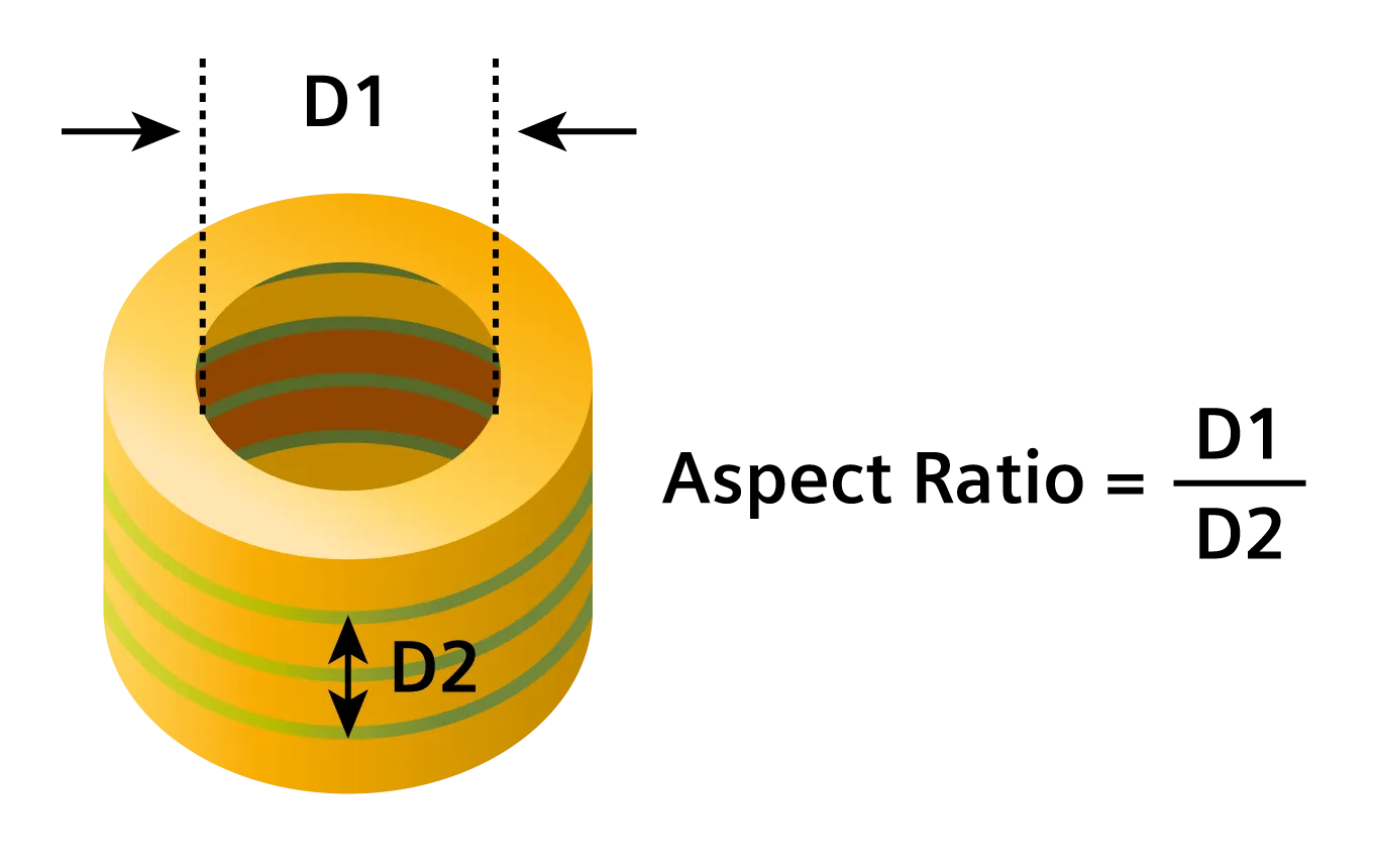
One of the most frequent EQs involves the Aspect Ratio, which is the ratio of the board thickness to the diameter of the smallest drilled hole. In thick FR4 designs, designers often attempt to use small vias (e.g., 0.2mm) on a 3.2mm board, resulting in a 16:1 ratio that exceeds standard plating capabilities. Our engineering team detects this during the DFM check by calculating whether our plating chemistry can reach the center of the hole to deposit a consistent copper barrel. If the aspect ratio is too high, the query will suggest increasing the hole size or reducing the board thickness to avoid the risk of open circuits or "barrel cracking" during thermal cycling. Failing to adjust this can lead to intermittent connectivity issues that are difficult to diagnose after the board is assembled.
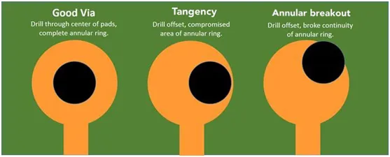
Drill wander and annular ring sufficiency represent another common area of concern for substrates with high thickness. Because thick boards require longer drill bits that are prone to deflection or "walking" as they penetrate the material, maintaining registration between layers becomes significantly harder. CAM engineers identify potential issues when the annular ring margins are too tight to accommodate the expected mechanical tolerances of deep drilling. We often issue an EQ to request permission to increase pad sizes or move nearby traces to prevent "breakout," where the hole exits the copper pad. Without these adjustments, the board faces a high risk of short-circuiting or compromised signal integrity due to misaligned vias.
Thermal relief design in thick FR4 PCBs frequently triggers queries regarding heat absorption during the soldering process. Because a thicker board acts as a larger heat sink, standard thermal relief pads with narrow bridges may prevent the solder from flowing properly, leading to cold solder joints. During engineering review, we check the connection width between pads and copper planes to ensure they are robust enough for the thermal mass of the board. An EQ is generated to suggest widening these bridges or modifying the relief pattern to guarantee a reliable solder bond. Ignoring this factor can result in components detaching or failing under mechanical stress because the solder did not achieve full wetting.
Main Causes of Engineering Queries in Thick FR4 PCB File Review
Most engineering queries regarding thick FR4 PCBs stem from a mismatch between CAD software default settings and the physical limitations of specialized fabrication. Designers often work with standard design rules intended for 1.6mm boards, which do not automatically account for the increased Z-axis expansion or the drilling mechanics of a 3.2mm or 6.0mm substrate. Furthermore, there is often a lack of communication regarding the final application's environment, which dictates whether a High Tg (Glass Transition Temperature) material is necessary to prevent delamination in thick boards. The CAM review is the first time these theoretical designs meet practical physics, where the factory must account for things like plating fluid dynamics and drill bit stability that aren't visible in a digital environment.
How to Reduce Engineering Queries in Thick FR4 PCB Design
To minimize EQs and keep your project on schedule, it is essential to design with the aspect ratio in mind from the very beginning. As a general rule, aim to keep your aspect ratio below 10:1; for a 3.2mm board, this means your smallest finished hole should be at least 0.35mm. Additionally, you should always specify a High Tg material for thick boards to manage the cumulative thermal expansion that occurs during multiple reflow cycles. Increasing the minimum annular ring by at least 20% over standard rules will also help accommodate drill wander, reducing the need for registration-related queries. Finally, providing a detailed stack-up and clearly stating the finished board thickness tolerance will allow our engineers to choose the best processing parameters without needing to stop for clarification.
Conclusion
Thick FR4 PCBs are robust solutions for demanding applications, but they require a higher level of DFM discipline than standard boards. By understanding the common engineering queries related to aspect ratios, drilling tolerances, and thermal management, you can create designs that flow through the factory with minimal delays. At AIVON, our goal is to partner with you to resolve these technical challenges before they become production bottlenecks. A well-prepared file not only ensures a faster turnaround but also guarantees the long-term reliability and performance of your thick-film electronics.
FAQs
Q1: What is the maximum aspect ratio AIVON can support for thick FR4 PCBs?
A1: While we can support aspect ratios up to 12:1 for specialized projects, we generally recommend staying below 10:1 for standard production to ensure optimal plating reliability. For boards thicker than 3.2mm, larger hole sizes are always preferred to facilitate chemistry flow.
Q2: Why do thick boards often require a High Tg material specification?
A2: Thick boards have more resin and reinforcement in the Z-axis, which leads to greater expansion when heated. High Tg materials (170°C or higher) have a lower Coefficient of Thermal Expansion (CTE), which prevents the via barrels from cracking during assembly or operation.
Q3: How does board thickness affect the finished hole size tolerance?
A3: As thickness increases, it becomes harder to maintain extremely tight hole tolerances due to the increased wear on drill bits and the challenge of uniform plating. We typically recommend a slightly wider tolerance (e.g., +/- 0.1mm) for holes in boards over 3.0mm thick.
Q4: Will a thicker FR4 board increase the lead time for my order?
A4: Yes, thick boards often require longer drilling cycles, slower plating times, and extended baking periods to remove moisture. Planning for an additional 2-3 days in the production schedule is common for substrates exceeding 2.5mm.
Reference
IPC-6012E — Qualification and Performance Specification for Rigid Printed Boards. IPC, 2017
IPC-2221B — Generic Standard on Printed Board Design. IPC, 2012