Introduction
In the realm of high-frequency electronics, standard FR-4 laminates have long served as the backbone for many printed circuit boards. However, as RF and microwave applications push beyond gigahertz frequencies, the limitations of FR-4 become evident due to its relatively high dielectric constant and dissipation factor. Advanced low Dk PCB laminates emerge as essential solutions for maintaining signal integrity in these demanding environments. These materials enable smaller, more efficient designs by supporting faster signal propagation and reduced losses. This article delves into the principles, types, and best practices for integrating low Dk PCB RF applications, drawing from established industry standards to guide electric engineers in microwave PCB design.
What Are Low Dk PCB Laminates and Why They Matter for RF Applications
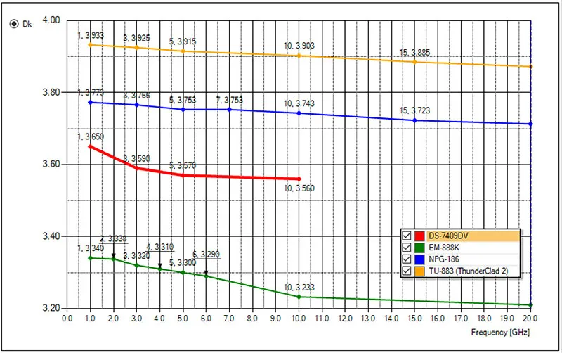
Low Dk PCB laminates refer to substrates engineered with a dielectric constant significantly lower than traditional FR-4, typically enabling better performance at high frequencies. The dielectric constant, or Dk, measures a material's ability to store electrical energy in an electric field, directly influencing signal speed and impedance control. In RF PCB laminates, a lower Dk reduces phase velocity variations, minimizing signal distortion over distance. This is critical for applications like radar systems, wireless communications, and satellite technology where even minor losses can degrade performance.
The dissipation factor, or Df, complements Dk by quantifying energy loss as heat during signal transmission. High-frequency PCB materials with low Df values preserve signal amplitude, ensuring reliable data transfer in microwave PCB design. Beyond electrical properties, these laminates address thermal and mechanical stability challenges inherent in FR-4 at elevated frequencies. Factory-driven insights emphasize selecting materials aligned with IPC-4103 specifications for high-speed and RF applications, guaranteeing consistency in production.
As frequencies exceed several gigahertz, FR-4's higher Dk leads to increased insertion loss and crosstalk, compromising overall system efficiency. Low Dk alternatives allow engineers to shrink circuit sizes while maintaining controlled impedance, optimizing space in compact devices. Ultimately, adopting these RF PCB laminates translates to enhanced reliability and performance in real-world deployments.
Key Technical Principles of Low Dk Materials in High-Frequency Applications
The core principle behind low Dk PCB RF applications lies in the relationship between dielectric properties and electromagnetic wave propagation. Signal velocity in a PCB trace is inversely proportional to the square root of the effective Dk, so lower values accelerate propagation and reduce delay skew between traces. This uniformity is vital for maintaining phase alignment in multi-layer stacks used in microwave circuits. Additionally, low Df minimizes attenuation, where energy dissipates as heat proportional to the tangent of the loss angle.
Temperature stability of Dk and Df is another critical factor, as thermal expansion can alter electrical characteristics during operation. Advanced high-frequency PCB materials incorporate reinforcements like glass fibers or ceramics to stabilize these properties across wide temperature ranges. Moisture absorption further impacts performance, with low Dk laminates designed to resist changes in Dk under humid conditions, per guidelines in relevant IPC standards.
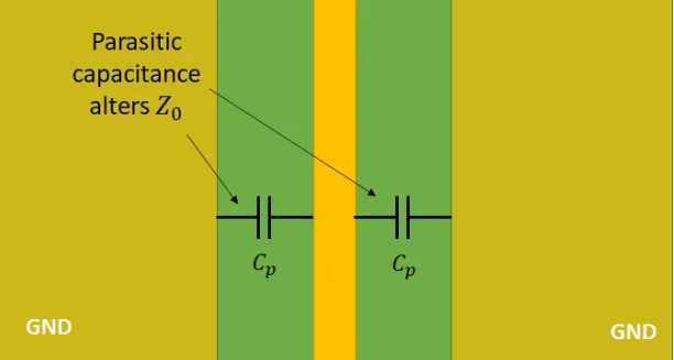
In microwave PCB design, the skin effect confines currents to trace surfaces at high frequencies, amplifying the need for smooth copper and low-loss dielectrics. Low Dk materials reduce capacitive coupling between adjacent traces, mitigating crosstalk in dense layouts. Engineers must model these interactions using field solvers to predict real-world behavior accurately.
Types of Advanced Low Dk Laminates for RF and Microwave Use
Several categories of low Dk PCB laminates cater to diverse RF needs, each with tailored compositions. Polytetrafluoroethylene, or PTFE, based laminates offer exceptionally low Dk and Df, ideal for pure microwave applications due to their non-polar nature. These materials often include ceramic fillers to enhance rigidity and thermal conductivity without compromising electrical performance.
Hydrocarbon ceramic laminates provide a balance of low loss and mechanical strength, suitable for hybrid circuits combining RF and digital signals. Polyphenylene ether resins deliver stable Dk over frequency, making them viable for high-volume production in low Dk PCB RF applications. Each type undergoes qualification per IPC-4103, which outlines specifications for base materials in high-frequency printed boards.
Glass-reinforced epoxies with modified resins represent a step beyond FR-4, offering lower Df for frequencies up to several gigahertz. Factory processes for these RF PCB laminates emphasize controlled resin content to achieve consistent dielectric uniformity. Selecting the appropriate type depends on operating frequency, power levels, and assembly compatibility.
Design Best Practices for Microwave PCB Using Low Dk Laminates
Effective microwave PCB design with low Dk materials starts with precise impedance control, targeting 50 ohms for most RF lines. Trace width and spacing calculations account for the lower Dk, often resulting in narrower traces than FR-4 designs. Microstrip and stripline configurations benefit from embedded dielectrics, reducing radiation losses. Adhering to IPC-2228 guidelines ensures sectional design standards for high-frequency printed boards, covering layout and via transitions.
Ground plane integrity is paramount, with solid pours minimizing return path inductance. Via fences or stitching provide low-impedance paths for RF currents, suppressing cavity resonances. Layer stacking optimizes signal-reference plane pairing to contain fields within low Dk regions. Simulation verifies these choices before fabrication.
Component placement prioritizes short RF paths, grouping sensitive circuits away from digital noise sources. Decoupling capacitors near IC pins stabilize power delivery without introducing parasitics. These practices, rooted in standard-aligned approaches, enhance yield in RF PCB laminates production.
Manufacturing Challenges and Solutions for High-Frequency PCB Materials
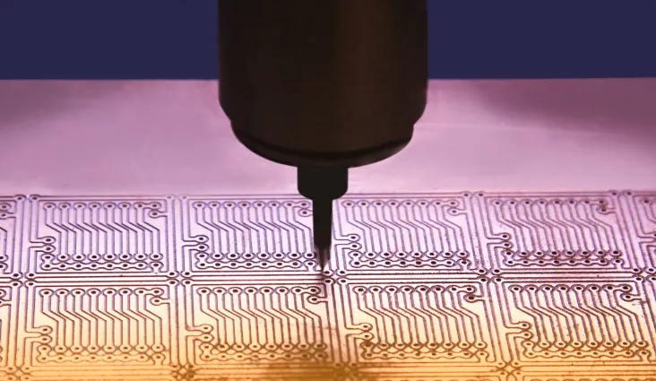
Fabricating PCBs with low Dk laminates introduces unique challenges due to their distinct material behaviors compared to FR-4. Drilling precision is critical, as PTFE variants exhibit stringy chips and require specialized carbide tools with high-speed peck cycles. Aspect ratios remain conservative to avoid via barrel defects, aligning with IPC-6018 qualification for high-frequency boards.
Copper plating demands low-etchback processes to preserve surface smoothness, reducing conductor losses. Lamination cycles adjust for lower flow resins, preventing voids in multi-layer builds. Thermal coefficient of expansion mismatches between laminate and copper necessitate controlled press parameters to minimize warpage.
Solder mask selection favors low-loss types compatible with high frequencies, applied thinly to avoid altering effective Dk. Electrical testing includes time-domain reflectometry for impedance verification and vector network analysis for insertion loss. Factory insights stress supplier qualification under IPC standards to ensure repeatability.
Case Insights: Optimizing RF Performance in Practice
Consider a typical phased array antenna module operating at microwave frequencies. Transitioning to low Dk PCB RF applications reduced phase errors by stabilizing signal paths, enabling beam steering accuracy. Design iterations focused on hybrid stacking, combining low Dk cores with cost-effective outer layers.
Troubleshooting common issues like via resonances involved adding radial stubs per IPC-2228 recommendations. Production scaling required moisture preconditioning to simulate field conditions, improving reliability. These factory-driven adjustments underscore the value of standards in bridging design and manufacturing.
Conclusion
Advanced low Dk PCB laminates represent a pivotal evolution beyond FR-4, unlocking superior performance in RF and microwave PCB design. By prioritizing low Dk and Df, engineers achieve precise control over signal propagation, integrity, and losses. Standards like IPC-4103, IPC-2228, and IPC-6018 provide the framework for selection, design, and qualification. Implementing best practices ensures robust outcomes in high-frequency PCB materials applications. As RF demands intensify, these materials will remain central to innovation in telecommunications and beyond.
FAQs
Q1: What makes low Dk PCB RF applications superior to FR-4 for microwave frequencies?
A1: Low Dk materials exhibit reduced dielectric constant and dissipation factor, minimizing signal attenuation and phase shifts at gigahertz levels. This supports controlled impedance and lower crosstalk in dense layouts. Factory processes align with IPC-4103 for consistent high-frequency performance, unlike FR-4's higher losses.
Q2: How do you select RF PCB laminates for a specific high-frequency design?
A2: Evaluate operating frequency, power, and thermal needs against material datasheets for Dk/Df stability. Prioritize IPC-2228-compliant designs for layout optimization. Balance cost with performance through hybrid stacks, ensuring manufacturability in microwave PCB design.
Q3: What are common manufacturing challenges with high-frequency PCB materials?
A3: Challenges include precise drilling, plating uniformity, and CTE matching to prevent warpage. Solutions involve specialized tools and controlled lamination per IPC-6018. Preconditioning for moisture enhances reliability in low Dk PCB RF applications.
Q4: Why is Df as important as Dk in Rogers PCB materials for RF?
A4: Low Df reduces energy dissipation as heat, preserving signal strength over distance. Combined with stable Dk, it ensures minimal insertion loss in high-frequency paths. Standards guide qualification for optimal microwave PCB design outcomes.
Reference
IPC-4103 — Specification for Base Materials for High-Speed/High-Frequency Printed Boards. IPC.
IPC-2228 — Sectional Design Standard for High Frequency (RF)/Microwave Printed Boards. IPC.
IPC-6018 — Qualification and Performance Specification for High Frequency (Microwave) Printed Boards. IPC.


