What Defines a Single-Layer PCB and Its Suitability for Simple Radio Circuits?
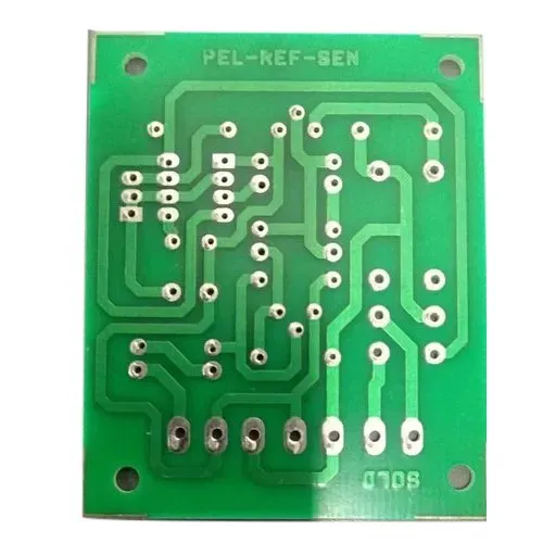
A single-layer PCB, often referred to as a single-sided printed circuit board, is characterized by having conductive traces exclusively on one side of the board. The opposing side is typically reserved for component mounting. These boards represent the most fundamental type of PCB, widely adopted in basic electronic applications due to their inherent cost-effectiveness and simplified manufacturing process. For a DIY radio project, a single-layer PCB presents an ideal solution, as it significantly reduces design complexity while still providing a robust and stable foundation for a basic receiver circuit.
Radio circuits, particularly elementary AM or FM receivers, frequently necessitate only a limited array of components, such as transistors, capacitors, and inductors. A single-layer PCB can readily accommodate these components without demanding the intricate routing associated with the multilayer PCB. Furthermore, single-sided PCB electronics are perfectly suited for beginners eager to delve into radio circuit PCB experimentation without the need for significant investment in advanced tools or specialized materials.
How Single-Layer Radio PCBs Work
To understand how a single-sided board supports a radio receiver, it is helpful to trace the signal flow across the physical layout. In a simple radio circuit, the operation follows a linear path that perfectly aligns with single-layer routing:
-
Signal Capture: An external wire antenna captures electromagnetic radio frequency (RF) waves from the air and channels them to the board.
-
Tuning (Filtering): The signal enters an LC circuit (a parallel inductor and variable capacitor). By adjusting the capacitor, the circuit resonates at a specific frequency, isolating the desired radio station from all other incoming signals.
-
Demodulation: The filtered high-frequency AC signal passes through a detector—typically a germanium diode—which rectifies the RF signal, stripping away the high-frequency carrier wave and leaving only the low-frequency audio signal.
-
Amplification: Because the resulting audio signal is incredibly weak, it is routed into a transistor amplifier stage.
-
Output: Finally, the amplified signal drives a small earphone or speaker.
Because this flow is largely sequential, a radio pcb design can be laid out linearly on a single layer without signal traces needing to cross over one another, ensuring minimal interference and straightforward assembly.
What Are the Advantages of Using a Single-Layer PCB for a Basic Simple Radio Receiver?
Before delving into the specifics of design and assembly, it is beneficial to understand why a single-layer PCB stands out as an excellent choice for constructing a basic radio receiver. Its straightforward construction offers a multitude of benefits, summarized in the table below:
| Feature | Advantage for Radio Circuits |
| Cost-Efficiency | Single-layer boards use less copper and require fewer manufacturing steps, making them the most economical option for prototyping a simple radio circuit. |
| Design Simplicity | Routing traces on a single plane eliminates the need for complex via management and layer-stack planning, lowering the barrier to entry for novice designers. |
| Reduced Crosstalk | With a well-planned linear layout, single-layer designs avoid the capacitive coupling that can sometimes occur between overlapping parallel traces on multilayer boards. |
| Ease of Troubleshooting | All components are on the top, and all traces are visible on the bottom. Tracing a short or a broken connection is visually immediate using a basic multimeter. |
| Rapid Prototyping | The sheer simplicity of the board allows for easy at-home etching or incredibly fast turnaround times from professional fabrication houses. |
What Components and Tools Are Needed for a Single-Layer PCB Radio?
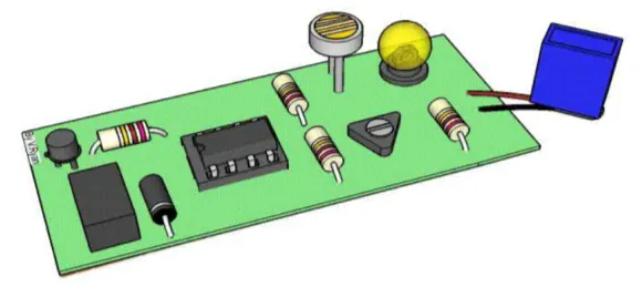
Constructing a basic receiver on a single-layer PCB requires a minimal selection of components and readily available tools. This project will focus on an elementary AM radio receiver, chosen for its straightforward design and ease of assembly.
Essential Electronic Components
-
Amplification: A general-purpose NPN transistor (e.g., 2N2222) to boost the audio signal.
-
Tuning Stage: A 365 pF variable capacitor and an inductor (approximately 220 μH). These can be purchased or hand-wound specifically for the AM band.
-
Biasing & Filtering: 1 kΩ and 10 kΩ resistors to bias the transistor; 100 nF ceramic and 10 μF electrolytic capacitors for signal coupling and filtering.
-
Signal Detection: A germanium diode (e.g., 1N34A). Germanium is preferred over silicon for its lower forward voltage drop (around 0.3V), which is critical for weak RF signals.
-
Peripherals: A 3–5 meter extended wire for the antenna, a 9V battery (with clip), and a high-impedance earphone (or 8-32 ohm small speaker).
Necessary Tools for Assembly
The PCB board assembly process requires a soldering iron and compatible solder wire. For initial design, PCB design software (with free options available online) is essential. A multimeter is crucial for testing connections and troubleshooting. Standard wire cutters and strippers will be needed for preparing component leads. If you plan to fabricate the PCB at home, a drill or an etching kit will also be necessary.
Radio PCB Design Guide: How to Design a Single-Layer PCB for a Radio Circuit
The initial phase in constructing your simple receiver PCB involves creating the layout. Given its single-layer nature, the design process is relatively straightforward, requiring the creation of a schematic which is then translated into a PCB layout with all conductive traces confined to one side.
Schematic Creation for an AM Receiver
Begin by drawing the schematic for a basic AM radio receiver. This circuit typically features an antenna connected to a tuned circuit, which comprises a parallel arrangement of an inductor and a variable capacitor. Following this, a detector stage, usually a diode, processes the signal, which is then fed into an amplifier stage utilizing a transistor. The final output is directed to an earphone or a small speaker. Employ free design software to clearly illustrate all connections. The tuned circuit is designed to resonate within the AM broadcast band, spanning 530 kHz to 1700 kHz. The relationship between inductance (L) and capacitance (C) for resonance is defined by the formula: f = 1/(2π√(LC)). For instance, a 220 μH inductor combined with a 365 pF capacitor allows tuning around 800 kHz at its midpoint.
Translating to a Single-Layer PCB Layout
Once the schematic is complete, proceed to convert it into a single-layer PCB layout. The primary goal is to place all components on one side of the board and route all conductive traces on the opposite side. It is advisable to keep traces as short as possible, particularly around the sensitive tuned circuit, to minimize potential interference. Ensure sufficient spacing between components to facilitate ease of soldering during assembly. For beginner projects, a 5x5 cm board generally provides adequate space for this simple receiver PCB design.
Assembling Your Single-Layer PCB Radio Circuit
With your PCB design finalized and the board either professionally fabricated or etched at home, the next crucial step is the assembly of the components. Adhering to these sequential steps will guide you towards a successful build.
PCB Preparation and Component Soldering
Begin by preparing your PCB. If you've received a professionally manufactured board, ensure it's clean and free from any residues. For home-etched boards, carefully inspect for any broken traces or unintended shorts using a multimeter, and drill any necessary holes for through-hole components. Proceed to solder the components, starting with the smallest ones like resistors and capacitors. Following these, attach the transistor and diode, paying close attention to their correct orientation as specified in their datasheets. Finally, solder the variable capacitor, inductor, and external connections such as the antenna wire and earphone jack. Throughout the soldering process, use a minimal amount of solder to prevent accidental bridges on this single-sided PCB electronics project.
Power Connection and Initial Testing
Once all components are securely soldered, connect the 9V battery or your chosen power source. Attach the antenna wire, ensuring it is extended to its maximum practical length for optimal signal reception. Power on the circuit and slowly adjust the variable capacitor to sweep through the AM band. You should begin to hear faint audio through the earphone. If there is no sound, systematically review all your connections, paying particular attention to the orientation of polarized components. If possible, use a multimeter to check the resonance of the tuned circuit to confirm its functionality.
Troubleshooting Common Issues with Your Single-Layer PCB Radio
It's not uncommon for a simple receiver PCB to not function perfectly on the first attempt. If your DIY radio doesn't work as expected, these troubleshooting tips can help diagnose and resolve common problems.
Resolving Signal and Connection Problems
If you experience no sound, first verify that the antenna connection is secure and that the antenna wire itself is sufficiently long, ideally between 3-5 meters. Double-check the orientation of the transistor and diode, as incorrect placement is a frequent cause of circuit failure. For a weak signal, consider adjusting the values of the inductor or capacitor within the tuned circuit to better align with the AM broadcast band (530-1700 kHz). Also, try relocating to an area with potentially stronger radio reception. If static or unwanted noise is present, evaluate whether shortening any PCB traces is feasible, as longer traces can act as antennas for ambient interference. Additionally, ensure all solder joints are clean, shiny, and free of cold joints or bridges that could introduce noise or break connections.
Enhancing Your Basic DIY PCB Radio Project
Once your fundamental single-layer PCB radio circuit is successfully operational, you might consider various upgrades to augment its performance and features.
Boosting Audio and Expanding Frequency Range
To achieve louder audio output, suitable for a small speaker rather than just an earphone, you could integrate an additional transistor amplifier stage or a compact audio amplifier IC into your circuit. If you wish to explore beyond the AM band, redesigning the tuned circuit for the FM band (88-108 MHz) would involve using a smaller inductor (around 0.1 μH) and capacitor (10-50 pF). Finally, constructing a custom enclosure for your PCB and components will not only provide protection but also enhance the device's portability and overall aesthetic appeal.
The Benefits of Professional PCB Fabrication for Simple Radio Circuits
While the home etching of a single-layer PCB is certainly an option, utilizing a professional fast turn PCB fabrication service offers significant advantages, especially for beginners. Professional services ensure the production of boards with precise traces, consistent quality, and enhanced durability—all critical factors for a reliable radio circuit PCB. Moreover, outsourcing fabrication allows you to easily order multiple copies of your simple receiver PCB, perfect for future projects or for sharing your creations with others.
Companies like AIVON specialize in delivering high-quality single-layer PCBs at competitive prices. Their user-friendly platforms typically allow you to effortlessly upload your design, review it, and then have your custom-made boards delivered promptly. Whether your endeavor is a DIY radio project or other single-sided PCB electronics, professional services support your creative pursuits with efficient turnaround times and exceptional customer service.
Conclusion: Launch Your Single-Layer PCB Radio Project Today
Embarking on the construction of a simple receiver using a single-layer PCB is an incredibly engaging and fulfilling DIY radio project. With just a handful of components and a thoughtfully designed radio circuit PCB, you possess the capability to tune into AM stations and simultaneously grasp fundamental electronic principles. Single-sided PCB electronics are ideally suited for beginners due to their inherent simplicity and cost-effectiveness, making them an outstanding choice for initial forays into basic radio circuit experimentation.
By diligently following the step-by-step instructions provided in this guide, you can confidently design, assemble, and troubleshoot your very own simple receiver PCB. Whether you are an enthusiastic hobbyist or a student keen on practical learning, this project promises invaluable hands-on experience with single-layer PCB radio design. Consider ordering your custom PCB today and take that exciting first stride towards bringing your personal radio receiver to life!
FAQs
Q1: Do I need a ground plane on a single-layer board?
A1: While multilayer boards rely heavily on dedicated ground planes for noise reduction, adding a full copper pour connected to ground on the bottom layer of your single-layer PCB is highly recommended. A ground pour helps shield the delicate RF signals from external electromagnetic interference, resulting in clearer audio reception.
Q2: What trace width is best for a DIY single-layer radio board?
A2: For this type of project, trace widths between 20 to 30 mils (0.5 to 0.76 mm) are ideal. While modern manufacturing can easily handle traces as thin as 4 mils, wider traces are highly recommended for single-layer boards. Thicker traces are much less prone to peeling off the fiberglass substrate if you accidentally apply too much heat with your soldering iron, making assembly much more forgiving for beginners.
Q3: Is a single-layer PCB suitable for FM radio circuits?
A3: Yes, but it requires much stricter design rules. Because FM operates at much higher frequencies (88–108 MHz) compared to AM, parasitic capacitance and trace inductance become major factors. Traces must be kept incredibly short, and the layout must minimize loops to prevent the circuit from detuning.


