Introduction
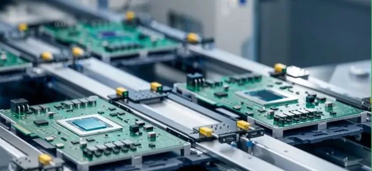
LED lighting PCBs drive efficient illumination in homes and industries. Mass production demands designs that cut costs without sacrificing performance. Engineers face challenges like heat dissipation and component density. Cost reduction strategies for LED PCBs start with smart material choices and layout tweaks. Minimizing material costs in LED PCB design involves selecting affordable substrates. Automated assembly for LED PCBs speeds throughput and lowers labor. Optimizing PCB panelization for LED lighting maximizes yield per panel. Design for manufacturability (DFM) in LED PCBs integrates factory realities early. From my assembly line experience, these steps prevent rework and boost margins. This article shares practical tips drawn from high-volume runs. It covers principles and solutions for reliable, economical boards. Teams gain troubleshooting insights to scale LED projects smoothly.
What Is Optimizing LED PCB Design for Mass Production and Why It Matters
Optimizing LED PCB design means refining layouts and specs for cost-effective scaling. It focuses on high yields in automated lines. Key elements include trace routing for current flow and pad sizing for pick-and-place.
This matters in LED lighting where volumes hit thousands. Poor designs inflate material waste and assembly errors. Factories see 10 to 20 percent yield drops from unoptimized panels. Cost reduction strategies for the custom LED PCB board address this head-on. They align with IPC-2221G generic standards for land pattern and spacing. Compliance ensures solder joint reliability under thermal loads.
In applications like streetlights, boards endure cycles of on-off stress. Minimizing material costs in LED PCB design preserves budget for optics. Automated assembly for LED PCBs cuts cycle times to seconds per unit. Optimizing PCB panelization for LED lighting fits more boards per sheet. DFM in LED PCBs flags issues like via placement early. Experience shows these tactics slash per-unit costs by optimizing flow from fab to pack.
Technical Principles of Cost Optimization in LED PCB Design
LED PCBs handle forward voltages from 2 to 3.5 volts per diode. Current paths demand low-resistance traces to avoid hotspots. Copper weight of 1 oz suits most designs, balancing cost and conductivity.
Material Selection Fundamentals
Substrates like PCB FR4 material provide dielectric strength at low expense. Thinner cores reduce weight for shipping savings. Solder mask thickness of 15 to 25 microns protects traces without excess buildup. IPC-6012DS w/amendment specifies qualifications for double-sided boards in lighting.
Thermal vias under LEDs channel heat to planes. Their diameter of 0.3 mm aids drilling efficiency. Surface finishes like HASL minimize costs for wave soldering compatibility.
Layout and Routing Mechanisms
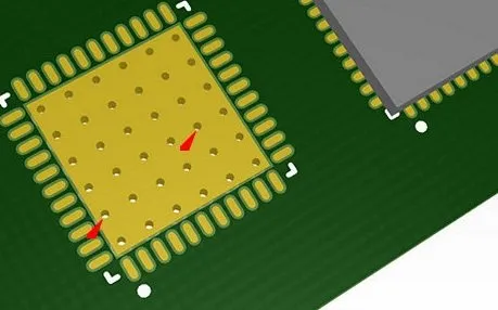
Component spacing follows 0.5 mm minima for automated assembly for LED PCBs. This prevents bridging in high-density arrays. Panelization principles group boards with V-grooves for clean depaneling. Optimizing PCB panelization for LED lighting uses nested patterns to fill 90 percent of sheet area.
Current sharing across parallel LEDs evens brightness. Trace widths scale with ampacity per IPC-2221G formulas. Design for manufacturability (DFM) in LED PCBs incorporates fiducials for alignment accuracy within 50 microns.
Practical Solutions and Best Practices
Implement cost reduction strategies for LED PCBs through iterative reviews. Start with Gerber checks for overlap errors. Use 1.6 mm thickness for standard FR4 to leverage stock availability.
Minimizing Material Costs in LED PCB Design
Select copper-clad laminates in bulk to drop per-square costs. Avoid gold fingers unless edge connectors demand them. Opt for matte green mask over specialty colors. Factories confirm these choices trim 15 percent from bills.
Layer counts stay at two for strip lights. This skips blind vias and sequential lamination. IPC-A-610F class 2 criteria guide joint inspections post-assembly.
Automated Assembly for LED PCBs
Position LEDs with 120-degree orientation for even reflow exposure. Pad designs per IPC-7351C ensure self-alignment during placement. Speeds reach 10,000 units per hour with dual-beam machines.
Program feeders for tape reels to avoid changeovers. Solder paste volume of 100 percent stencil aperture fills prevents voids. Experience highlights flux selection for no-clean processes to eliminate wash steps.
Optimizing PCB Panelization for LED Lighting
Array boards in 18 by 24 inch panels. Rail widths of 10 mm support handling bars. Tab connections of 2 mm thickness ease breakout without burrs.
Test depaneling forces under 50 N to protect traces. This setup yields 20 boards per panel for linear designs.
Design for Manufacturability (DFM) in LED PCBs
Incorporate 5 mm borders for clamping. Route traces away from edges to dodge stress cracks. Simulate thermal profiles with finite element tools before fab.
Review DFM checklists for annular ring minima of 75 microns. These practices cut scrap from 5 percent to under 1 percent in runs.
Practical Summary Table
This table outlines quick wins. Inline AOI verifies post-etch integrity.
| Strategy | Benefit | Implementation Tip |
|---|---|---|
| Material Minimization | 10-15% cost drop | Use 1 oz copper, standard FR4 |
| Automated Assembly | Faster throughput | 0.5 mm spacing, fiducials |
| Panelization Optimization | Higher yield per sheet | V-grooves, 90% utilization |
| DFM Integration | Fewer defects | Pre-fab simulations, IPC checks |
Troubleshooting Insights from Assembly Experience
High-volume LED lines reveal common pitfalls. Overcrowded pads cause tombstoning in reflow. Solution: Extend pads 0.1 mm beyond component footprints per IPC-7351C.
Panel warpage from uneven copper skews placement. Balance pours across layers to stay under 0.75 percent bow. Circuit board cost reduction strategies for LED PCBs falter here without checks.
Solder beads from excess paste mar optics. Stencil apertures at 100 to 120 percent resolve this. In one run, minimizing material costs in LED PCB design overlooked via plating. This led to opens; switching to tented vias fixed it.
Automated assembly for LED PCBs jams on bent leads. Pre-form components and add vision correction. Optimizing PCB panelization for LED lighting ignores fiducial count, risking misalignment. Place three per corner for sub-25 micron accuracy.
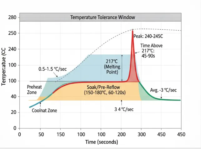
DFM in LED PCBs skips thermal testing, inviting hotspots. Bake prototypes at 85 degrees Celsius for two hours to mimic aging. These fixes, rooted in daily shifts, save thousands in rework.
Suggested Reading: Designing for Batch Assembly: Best Practices for Component Placement
Conclusion
Optimizing LED lighting PCB design unlocks cost-effective PCB mass production. Cost-reduction strategies for LED PCBs rely on wise integration of materials and manufacturing processes. Minimizing material costs in LED PCB design, combined with automated assembly, supports consistent quality at scale. Optimized PCB panelization for LED lighting further improves throughput and yield in mass production environments. Design for manufacturability (DFM) ties all these elements together, enabling stable, high-volume PCB mass production. Assembly experience confirms that these approaches deliver durable, high-brightness boards while controlling costs. Applying them helps manufacturers reduce expenses and scale reliably, while future LED PCB designs will increasingly leverage simulation tools to further optimize performance and mass production efficiency.
FAQs
Q1: What cost reduction strategies for LED PCBs work best in high-volume lighting?
A1: Focus on FR4 substrates and 1 oz copper to lower raw expenses. Balance copper distribution for flat panels. Use V-groove panelization to fit more units. From assembly floors, these cut waste by streamlining depaneling. IPC-2221G guides trace sizing for current efficiency. This keeps per-board costs under target without dimming output.
Q2: How can minimizing material costs in LED PCB design maintain thermal performance?
A2: Choose 1.6 mm FR4 with thermal vias under pads. Limit layers to two for simple heat paths. Avoid thick masks that trap warmth. Practical runs show tented vias reduce plating needs while aiding dissipation. Follow IPC-6012DS for qualification. These tweaks preserve reliability at budget levels for strip applications.
Q3: Why prioritize automated assembly for LED PCBs in mass production?
A3: It handles SMD placement at high speeds with low error rates. Standardize footprints per IPC-7351C for seamless pick-and-place. Add fiducials to correct offsets. Experience confirms no-clean flux skips cleaning stations. This shortens cycles and fits optimizing PCB panelization for LED lighting. Yields climb to 99 percent in optimized lines.
Q4: How does design for manufacturability (DFM) in LED PCBs prevent production delays?
A4: DFM reviews flag spacing violations early. Simulate reflow to catch tombstoning risks. Specify rail tabs for handling. Troubleshooting sessions reveal annular rings below 50 microns cause drills to wander. Adhere to IPC-A-610F for joint criteria. This upfront work avoids costly stops in automated assembly for LED PCBs.
References
IPC-2221G — Generic Standard on Printed Board Design. IPC, 2012.
IPC-6012DS w/amendment 1 — Qualification and Performance Specification for Rigid Printed Boards for Space and Military Applications. IPC, 2007.
IPC-7351C — Generic Requirements for Surface Mount Design and Land Pattern Standard. IPC, 2010.
IPC-A-610F — Acceptability of Electronic Assemblies. IPC, 2014.


