Introduction
Fitness trackers rely on compact PCBs to integrate multiple sensors for monitoring activity, heart rate, and other vital signs. These devices demand ultra-low power consumption to extend battery life over days or weeks without frequent charging. Sensor interface design PCB wearables becomes critical, as inefficient interfaces can drain batteries quickly despite advanced sensors. Engineers must balance signal integrity, noise reduction, and power efficiency in the analog front-end. This article explores structured approaches to designing these interfaces, focusing on low power ADC fitness tracker implementations and signal conditioning circuits. By adhering to established principles, designers achieve reliable performance in constrained form factors.
Understanding Sensor Interfaces in Fitness Tracker PCBs
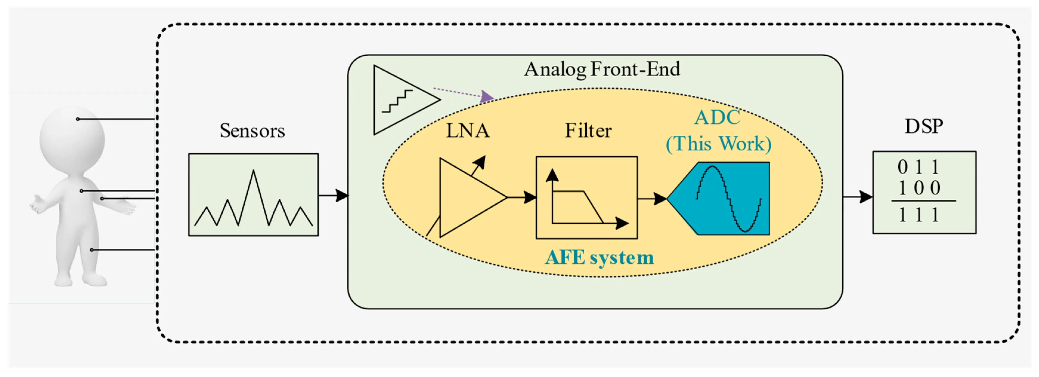
Sensor interfaces in fitness trackers connect physiological and motion sensors to the microcontroller or processor on the PCB. Common sensors include accelerometers for step counting, photoplethysmography (PPG) for heart rate detection, and temperature sensors for skin monitoring. These produce weak analog signals prone to noise from body movement or electromagnetic interference. The interface typically includes amplification, filtering, and digitization stages before data processing. Why does this matter for electric engineers? Poorly designed interfaces lead to inaccurate readings, increased power draw, and shortened device lifespan, undermining user trust in fitness data.
In wearables, PCB constraints amplify challenges: limited space favors flexible or rigid-flex boards, while battery sizes remain small. Interfaces must support duty-cycled operation, where sensors activate intermittently to conserve energy. Signal conditioning circuits prepare raw sensor outputs for accurate analog-to-digital conversion, ensuring high resolution despite low sampling rates. Low power ADC fitness tracker designs prioritize successive approximation register (SAR) architectures over higher-power alternatives like sigma-delta for intermittent use. Overall, effective sensor interface design PCB wearables directly impacts device competitiveness through superior battery life and data fidelity.
Core Technical Principles of Ultra-Low Power Sensor Interfaces
The foundation of ultra-low power sensor interfaces lies in minimizing static and dynamic power across the signal chain. Sensors output millivolt-level signals requiring amplification without introducing offset or noise. Signal conditioning circuits employ instrumentation amplifiers with high common-mode rejection to isolate bio-signals from motion artifacts. Low-pass filters follow to prevent aliasing during ADC sampling, using passive RC networks or active Sallen-Key topologies for power efficiency. Engineers select components with picoampere bias currents to reduce quiescent power, critical for always-on monitoring.
Analog-to-digital conversion represents a major power bottleneck, so low power ADC fitness tracker choices emphasize SAR converters operating at sub-1 MSPS with 10-16 bit resolution. These ADCs use charge redistribution, consuming power mainly during conversion cycles rather than continuous operation. Power scaling features allow dynamic adjustment of reference voltage or sampling rate based on activity levels. In PCB layout, analog and digital grounds separate via split planes to prevent noise coupling, joined at a single point under the ADC. Compliance with IPC-6013 ensures flexible PCB sections withstand repeated bending without degrading interface performance.
Power management integrates low-dropout regulators (LDOs) or switched-capacitor DC-DC converters tailored for sensor supplies. These maintain clean rails despite load transients from sensor activations. Event-driven architectures trigger interfaces only on motion detection, slashing average power by over duty cycle ratios. Thermal management prevents self-heating in dense layouts, as elevated temperatures degrade sensor accuracy and accelerate battery aging.
Signal Conditioning Circuits: Key to Reliable Data Acquisition
Signal conditioning circuits form the bridge between raw sensor outputs and the ADC input. For PPG sensors, transimpedance amplifiers convert photodiode currents to voltages, followed by bandpass filters to isolate pulse waveforms. Accelerometer interfaces use differential amplifiers to amplify capacitive changes, rejecting common-mode noise from vibrations. In fitness trackers, multi-channel conditioning shares components via multiplexers, reducing footprint and power. Engineers optimize gain staging to match dynamic ranges, avoiding saturation during high-activity periods.
Noise mitigation dominates design: shielding traces with ground pours and using twisted pairs for off-board sensors minimizes electromagnetic pickup. Anti-aliasing filters with cutoff frequencies below Nyquist rates ensure clean spectra. Low power op-amps with chopper stabilization eliminate 1/f noise without excessive bandwidth. PCB routing keeps analog paths short and symmetric, with guard rings around sensitive nodes. These practices maintain signal-to-noise ratios above 60 dB, vital for extracting heart rate variability.
For bio-potential sensors like ECG add-ons, right-leg drive circuits cancel common-mode voltages from body impedance. High-input impedance buffers prevent loading weak sources. Power gating isolates unused channels, dropping leakage to nanoamperes. Testing verifies conditioning under flexed PCB conditions per IPC-2223 guidelines for interconnect reliability.
Best Practices for PCB Implementation
Start with stackup selection: four-layer rigid-flex boards provide dedicated analog planes while supporting bend zones. Place sensors near conditioning circuits to shorten traces, reducing parasitic capacitance. Decoupling capacitors, sized 0.1 μF and 10 μF, ride every supply pin with vias to inner planes. Digital signals cross analog sections at 90 degrees to avoid coupling.
Component selection favors QFN or WLCSP packages for thermal efficiency and low inductance. Firmware optimizes sampling: adaptive rates drop during inactivity, using threshold-based wakeups. Simulate power budgets with SPICE models, targeting microampere averages. For assembly, follow J-STD-001 requirements to avoid flux residues that boost leakage.
Validation includes bench testing with oscilloscopes for settling times and spectrum analyzers for noise floors. Flex cycling tests confirm interface stability. Iterate layouts to balance EMI compliance and power integrity.
Common Challenges and Troubleshooting Insights
Motion artifacts plague PPG accuracy; counter with adaptive filtering or multi-wavelength LEDs. ADC nonlinearity from reference drift resolves via external precision references or ratiometric sensing. Battery droop under load triggers brownouts, mitigated by reservoir capacitors. Flex-induced microcracks degrade traces; IPC-6013 qualification catches these early.
Debug systematically: scope ADC inputs during flexing, measure leakage currents, and profile power with ammeters. Firmware logs correlate data drops to power states.
Conclusion
Designing ultra-low power sensor interfaces for fitness tracker PCBs demands integrated thinking across analog design, PCB layout, and firmware. Signal conditioning circuits and low power ADC fitness tracker elements enable precise monitoring with minimal energy use. Adhering to standards like IPC-6013 and J-STD-001 ensures reliability in dynamic wearables. Engineers achieve extended battery life and robust performance by prioritizing noise isolation, efficient conversion, and optimized layouts. These principles position devices for market success in the competitive wearables space.
FAQs
Q1: What are the main considerations in sensor interface design PCB wearables for low power operation?
A1: Engineers focus on minimizing quiescent currents in amplifiers and ADCs, using duty cycling, and separating analog-digital domains on the PCB. Flexible layouts reduce parasitics, while event-driven triggers limit active time. Standards like IPC-6013 guide flex reliability. This approach extends battery life without sacrificing signal quality.
Q2: How does a low power ADC fitness tracker improve device efficiency?
A2: SAR ADCs excel in intermittent sampling, consuming power only during conversions with scalable resolution. Paired with efficient signal conditioning circuits, they handle low-frequency bio-signals effectively. PCB decoupling and short traces enhance performance. Firmware adjusts rates dynamically for optimal power.
Q3: Why are signal conditioning circuits essential in fitness tracker PCBs?
A3: They amplify weak sensor signals, filter noise, and match impedances for ADC input. Instrumentation amps reject motion artifacts, while anti-aliasing prevents distortion. Low-power designs use chopper amps for offset cancellation. Proper PCB routing maintains integrity in compact wearables.
Q4: What PCB layout tips optimize ultra-low power sensor interfaces?
A4: Use split ground planes joined at the ADC, place decoupling near pins, and shield analog traces. Rigid-flex stackups support bending without signal loss. Compliance with IPC-2223 ensures interconnect durability. These reduce noise and leakage for better efficiency.
References
IPC-6013DS — Qualification and Performance Specification for Flexible and Rigid-Flex Printed Boards. IPC, 2014
IPC-2223C — Sectional Design Standard for Flexible/Rigid-Flexible Printed Boards. IPC, 2019
J-STD-001H — Requirements for Soldered Electrical and Electronic Assemblies. IPC, 2020


